Traditionally, EMC has been regarded as "black magic." In fact, EMC can be understood by mathematical formulas. However, even if there are mathematical analysis methods available, those mathematical equations are still too complicated for the actual EMC circuit design. Fortunately, in most practical work, engineers do not need to fully understand the complicated mathematical formulas and the theoretical basis that exist in the EMC specification, as long as they can understand how to meet EMC requirements through a simple mathematical model. .

1. Wires and PCB traces
The seemingly inconspicuous elements such as wires, traces, holders, etc., are often the best emitters of RF energy (ie, the source of EMI). Each type of device has an inductance, which includes bond wires for silicon wafers, and pins for resistors, capacitors, and inductors. Each wire or trace contains hidden parasitic capacitances and inductances. These parasitic elements affect the impedance of the wire and are sensitive to frequency. Depending on the value of the LC (determining the self-resonant frequency) and the length of the PCB traces, self-resonance can be generated between a component and the PCB trace, thus forming an efficient radiating antenna.
At low frequencies, the wires are generally only resistive. However, at high frequencies, the wire has an inductive characteristic. Because of the high frequency, it will cause the change of the impedance, and then change the EMC design between the wire or the PCB trace and the ground. In this case, the ground plane and the ground grid must be used.
The main difference between wires and PCB traces is that the wires are round and the traces are rectangular. The impedance of the wire or trace includes the resistance R and the inductance XL = 2Ï€fL. At high frequencies, this impedance is defined as Z = R + j XL j2Ï€fL, and there is no capacitive reactance Xc = 1/2Ï€fC. When the frequency is higher than 100 kHz, the inductive reactance is greater than the resistance. At this time, the wire or trace is no longer a low-resistance connecting wire, but an inductance. In general, wires or traces that work above audio should be considered as inductors and cannot be seen as resistors, and they can be RF antennas.
The length of most antennas is equal to 1/4 or 1/2 wavelength (λ) of a particular frequency. Therefore, in the EMC specification, wires or traces are not allowed to operate below a certain frequency of λ/20, because this will suddenly make it a highly efficient antenna. Inductors and capacitors can cause resonance in the circuit. This phenomenon is not documented in their specifications.
For example, suppose there is a 10 cm trace, R = 57 mΩ, 8 nH/cm, so the total inductance is 80 nH. At 100 kHz, an inductive reactance of 50 mΩ can be obtained. When the frequency exceeds 100 kHz, the trace becomes an inductor and its resistance is negligible. Therefore, this 10 cm trace will form an efficient radiating antenna at frequencies above 150 MHz. Because at 150 MHz, its wavelength λ = 2 meters, so λ/20 = 10 cm = the length of the trace; if the frequency is greater than 150 MHz, its wavelength λ will become smaller, and its 1/4λ or 1/2λ will be Close to the length of the trace (10 cm), it gradually formed a perfect antenna.
2. Resistance
Resistance is the most common component on the PCB. The material of the resistor (carbon synthesis, carbon film, mica, winding, etc.) limits the effect of frequency response and the effect of EMC. Wirewound resistors are not suitable for high frequency applications because there is too much inductance in the wire. Although carbon film resistors include inductance, they are sometimes suitable for high frequency applications because the inductance of their pins is not large.
What people often overlook is the package size and parasitic capacitance of the resistor. Parasitic capacitance exists between the two terminals of the resistors, and they can damage the normal circuit characteristics at extremely high frequencies, especially when the frequency reaches GHz. However, for most application circuits, the parasitic capacitance between the resistor pins will not be more important than the pin inductance.
When the resistor is subjected to the overvoltage stress test, attention must be paid to changes in the resistance. If an "electrostatic discharge (ESD)" phenomenon occurs on the resistor, something interesting happens. If the resistor is a surface mount component, the resistor is likely to be penetrated by the arc. If the resistor has a pin, ESD will find the resistor's high-resistance (and high-inductance) path and avoid entering the circuit protected by this resistor. Actually, the true protector is the inductive and capacitive characteristics hidden by this resistor.
3 capacitance
The capacitor is generally applied to a power bus to provide decoupling, bypass, and maintenance of a fixed DC voltage and bulk. A truly simple capacitor will maintain its capacitance until it reaches the self-resonant frequency. Beyond this self-resonant frequency, the capacitance characteristics will become the same as the imaging inductance. This can be illustrated by the formula: Xc=1/2πfC, where Xc is the capacitive reactance (the unit is Ω). For example: a 10μf electrolytic capacitor with a capacitive reactance of 1.6Ω at 10 kHz and 160μΩ at 100 MHz. So at 100 MHz, there is a short circuit effect, which is ideal for EMC. However, the electrolytic capacitor's electrical parameters, equivalent series inductance (ESL) and equivalent series resistance (ESR), will limit the capacitor's ability to operate below 1 MHz. The use of capacitors is also related to the pin inductance and volume structure. These factors determine the number and size of parasitic inductances. Parasitic inductance is present between the wires of the capacitor, which causes the capacitor to behave as if it were above the resonant frequency. The capacitor therefore loses its previously set function.
4. Inductor
The inductor is used to control the EMI inside the PCB. For inductors, its inductive reactance is proportional to the frequency. This can be illustrated by the formula: XL = 2πfL, where XL is the inductive reactance (the unit is Ω). For example: An ideal 10 mH inductor with an inductance of 628 Ω at 10 kHz and 6.2 MΩ at 100 MHz. So at 100 MHz, this inductance can be seen as an open circuit. At 100 MHz, letting a signal pass through this inductor will result in a degradation of the signal quality (this is observed from the time domain). Like the capacitor, the electrical parameters of this inductor (parasitic capacitance between the coils) limit the inductance to work only at frequencies below 1 MHz.
The problem is, if you can't use an inductor at high frequencies, what would you use? The answer is that ferrite bead should be used. Iron powder materials are iron-magnesium or iron-nickel alloys. These materials have a high permeability, and at high frequencies and high impedance, the capacitance between the coils in the inductor is minimized. Iron powder beads are generally only suitable for high-frequency circuits, because at low frequencies, they are essentially full of inductance (including resistance and resistance components), and therefore cause slight losses on the line. At high frequencies, it basically has only the resistance component (jωL), and the resistance component increases with frequency, as shown in Figure 1. In fact, iron powder beads are high-frequency attenuators of RF energy.
In fact, iron powder beads can be considered as a resistor in parallel with an inductor. At low frequencies, the resistance is “shorted†by the inductor and the current flows to the inductor; at high frequencies, the high inductance of the inductor forces the current to the resistor.
In essence, iron powder beads are "dissipative devices" that convert high-frequency energy into heat energy. Therefore, in terms of performance, it can only be interpreted as a resistor, not an inductor.

5. Transformer
The transformer is usually present in the power supply. In addition, it can be used to insulate data signals, I/O connections, and power interfaces. Depending on the transformer type and application, there may be shields between the primary and secondary coils. This shield is connected to a grounded reference source to prevent capacitive coupling between the two sets of coils.
Transformers are also widely used to provide common mode (CM) insulation. These devices magnetically couple the primary side coil and the secondary side coil in accordance with a differential mode (DM) signal through its input to transfer energy. As a result, the CM voltage through the primary side coil is rejected, thereby achieving the purpose of common mode insulation. However, when the transformer is manufactured, there is a signal source capacitor between the primary and secondary coils. As the frequency of the circuit increases, the capacitive coupling capability also increases, thereby destroying the insulation effect of the circuit. If there is enough parasitic capacitance, high-frequency RF energy (from fast transients, ESD, lightning strikes, etc.) may pass through the transformer, causing the circuit on the other side of the insulation layer to receive this transient high Voltage or high current.
The above has been explained in detail for the hidden features of various passive components. The following will explain why these hidden features cause EMI in the PCB.
6. Talking about electromagnetic theory
The above-mentioned passive components have hidden characteristics and generate RF energy in the PCB, but why is this happening? In order to understand its origin, one must understand the Maxwell equation. Maxwell's four equations illustrate the relationship between electric and magnetic fields, and they are inferred from Ampere's law, Faraday's law, and Gauss's law. These equations describe the characteristics of electromagnetic field strength and current density in a closed loop environment and require the use of higher calculus to calculate. Because the Maxwell equation is very complex, only a brief explanation is given here. In fact, PCB cabling engineers do not need to fully understand the detailed knowledge of Maxwell's equations. As long as they understand the key points, EMC design can be completed. The complete Maxwell equation is as follows:
First law: Electric flux (from Gauss's law)

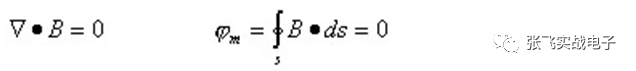
The second law: magnetic flux (from Gauss' law)
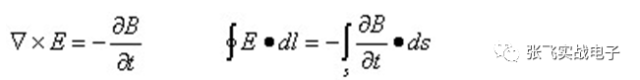
The third law: electric potential (from Faraday's law)
The fourth law: electric current (from Ampere's law)

In the above equation, J, E, B, H are vectors. In addition, the basic physical concepts related to the Maxwell equation are:
The Maxwell equation illustrates the interaction between charge, current, magnetic field, and electric field.
• The "Lorentz force" can be used to describe the physical force exerted by an electric field and a magnetic field on a charged particle.
â— All substances have a compositional relationship with other substances. This includes:
1. Conductivity: The relationship between current and electric field (Ohni's law of matter): J=σE.
2. Magnetic permeability: The relationship between magnetic flux and magnetic field: B = μH.
3. Dielectric constant: The relationship between charge storage and an electric field: D = εE.
J = Conduction current density, A/m2
σ = conductivity of the material,
E = electric field strength, V/m
D = flux density, coulombs / m2
ε = permittivity, 8.85 pF/m
B = flux density, Weber/m2 or Tesla
H = magnetic field, A/m
μ= Magnetic permeability of media, H/m
According to Gauss' law, Maxwell's first equation is also called "divergence theorem." It can be used to explain the electrostatic field E generated due to the accumulation of electric charge. This phenomenon is best observed between two boundaries: conductive and non-conductive. According to Gauss's law, behavior under boundary conditions creates a conductive cage (also known as a Faraday cage) that acts as an electrostatic shield. In an enclosed area surrounded by a Faraday box, electromagnetic waves around the outside cannot enter this area. If there is an electric field in the Faraday box, the electric charge generated by this electric field is concentrated on the inside of the boundary at its boundary. Charge outside the boundary is rejected by the internal electric field.
Maxwell's second equation shows that there is no magnetic charge in nature and only charge exists, that is, no single magnetic pole exists. Although the current Unified Theory theory predicts that there are few magnetic charges, it has not been proved so far in experiments. These charges are positively or negatively charged. Magnetic fields are generated by the action of electric currents and electric fields. Due to the current and electric field emission, they become the source of radiant energy. The magnetic field forms a closed loop around the current, and the magnetic field is generated by the current.
Maxwell's third-party program, also known as the "Faraday's Law of Induction," shows that when a magnetic field surrounds a closed circuit, the magnetic field will cause a current in the closed circuit. The third-party program and the fourth equation are accompanied. Third-party programs indicate that a changing magnetic field generates an electric field. Magnetic fields usually exist in transformers or coils, such as motors, generators, etc. The interaction of the third and fourth equations is EMC's main focus. Together, they illustrate how coupled electric and magnetic fields radiate or propagate at the speed of light. This equation also illustrates the concept of "skin effect", which predicts the effectiveness of "magnetic shielding." In addition, it also describes the characteristics of the inductor, which allows the antenna to be reasonably present.
Maxwell's fourth equation is also called Ampere's law. This equation illustrates two sources of magnetic field production. The first source is that the current is flowing in the form of transfer charges. The second source is that when the changing electric field surrounds a closed circuit, a magnetic field is generated. These sources of electricity and magnetism explain the effects of inductance and electromagnetics. In this equation, J represents the component of the magnetic field generated by the current;  It is the electric field that produces the component of the magnetic field.
7. Sources of electricity and magnetism
As mentioned earlier, the changing current generates a magnetic field, and the static charge distribution generates an electric field. The relationship between the current and the radiated electric field will be further discussed below. We must examine the structure of the current source and observe how it affects the radiation signal. In addition, we must also pay attention to the fact that the farther away from the current source, the lower the signal strength.
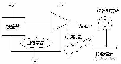
Time-varying currents exist in two structures: 1. Magnetic sources (closed loops), 2. Sources of electricity (dipole antennas). First discuss the source of magnetism.
8. Conclusion
As with most electronic engineering designs, EMC design requires careful consideration. At the time of reading this article, readers should refer to the EMC practice that is usually performed at the same time. This may lead to the discovery of many places that have not been noticed in the past, and these places are often the places where EMI is most likely to occur.
In an era that emphasizes the rapid availability of products, the pressure on engineers is increasing day by day. Although the use of good EMI simulation tools can help us to quickly achieve the task, if we rely too much on these tools, I am afraid that in some very special circumstances or circumstances, we can't do anything wrong. Therefore, having a solid theoretical foundation will make up for the lack of normal practice.
Ningbo Autrends International Trade Co.,Ltd. , https://www.mosvapor.com