Abstract: Design a PWM power supply for simulating the working state of automotive solenoid valve. The power supply is controlled by single-chip microcomputer. DDS chip AD9851 and PWM control chip SG3525 are used as waveform generating devices. Keyboard and liquid crystal display are used as human-machine interface. Output frequency The PWM signal can be arbitrarily set and displayed in real time from O to 25 000 Hz with a duty ratio of 0 to 100% and an amplitude in the range of 0 to 36 V. The power supply has stable operation and high precision, and has been successfully commissioned to the automobile and solenoid valve manufacturing enterprises.
Key words: solenoid valve; PWM; single chip microcomputer; DDS
Solenoid valves are widely used in modern automobiles, and the performance of solenoid valves is closely related to the performance of automobiles. The state of the power applied to the solenoid valve during actual operation is extremely complicated, mainly manifested in the voltage amplitude, frequency, duty cycle complexity and randomness of the solenoid valve power supply. In order to ensure the quality of the solenoid valve factory, this paper designs and produces a power supply that is convenient for simulating the actual working state of the automotive solenoid valve. According to the working requirements of the solenoid valve in the car, the quality requirements of the solenoid valve under various working conditions are simulated. At the same time, it solves the problem of testing the performance index of the export solenoid valve products, and provides the necessary technical performance testing equipment for the export products of China's solenoid valves.
1 System structure and working principle As shown in Figure 1, the whole system includes single chip microcomputer, I/O expansion circuit, D/A conversion circuit, PWM generation circuit, frequency selection circuit, photoelectric isolation and driving circuit, keyboard and display circuit. The system takes the single-chip microcomputer as the control center, adopts the DDS chip AD9851 and the PWM control chip SG3525 as the waveform generating device, and adopts the 8255A extended single-chip peripheral interface as the data input port of the three-way D/A conversion circuit. The three analog voltages are used to control the frequency and occupy the frequency respectively. Air ratio and amplitude. The frequency and duty ratio of the output signal of the waveform-generating device are processed by the single-chip microcomputer, and the PWM signal with adjustable output frequency, duty cycle and amplitude is realized by the frequency selection circuit and the optocoupler isolation and driving circuit of the latter stage. In addition, the human-machine interface uses a keyboard and LCD display, and is communicated by the PC after being communicated through the RS 232 serial port. 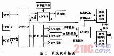
2 Signal generation and control circuit design system requires PWM signal with adjustable duty cycle between 0 and 25 000 Hz. PWM signal control chip SG3525 can easily generate PWM signal with independent adjustment of frequency and duty cycle. However, since the SG3525 is extremely unstable at frequencies below 150 Hz, it is necessary to design the signal into two frequency segments, wherein the low frequency band is 0 to 200 Hz, and the AD9851 is used as the signal generator, and the high frequency band is 200 to 25 000 Hz. The SG3525 is used as a signal generator.
2.1 Low-band PWM signal generation circuit The AD9851 is a highly integrated direct digital frequency synthesizer with controlled bandwidth, frequency and phase. Its main components are: phase accumulator, phase adder, waveform memory, digital multiplier and D/A converter. The basic work is: under the control of the sampling clock signal, the phase accumulator outputted by the frequency code outputs the phase code, and the waveform quantized sample data value stored in the read-only memory is read according to a certain rule, and is D/A converted. And low-pass filtering to output a sinusoidal signal.
The low-band signal generation circuit is shown in Figure 2. In the design circuit, the AD9851 externally connects a 30 MHz active crystal oscillator as the reference frequency source. The single-chip microcomputer and the AD9851 adopt the high-speed parallel interface working mode, and the pins P1.0~P1.7 of the AT89C55 are used as the parallel data input port of the AD9851, P2. O, P2.1, and P2.2 are used as I/O port output data to control the RESET, FQ_UD, and W_CLK of the AD9851. The AD9851 output frequency variable square wave is sent to the external interrupt INT0 of the microcontroller, and P2.3 is the low frequency PWM signal output port. The specific input mode of the MCU is: the valid reset signal RESET causes the input data address pointer to point to the first input register, the W_CLK rising edge writes the first group of 8-bit data, and the pointer points to the next input register. The input of all 40 bits of control data is completed by five consecutive W_CLK rising edges. Thereafter, the rising edge of the WCLK signal is invalid. When the rising edge of FQ_UD comes, the 40-bit control data is written into the frequency by the input register, the phase control register, the output frequency and phase are updated, and the address pointer is reset to the first input register, waiting for the next set of new data to be written. 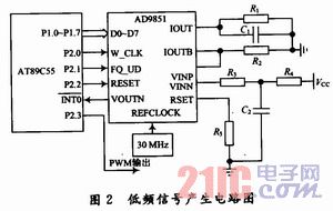
The AD9851 first outputs a pure sinusoidal signal through the IOUT pin. After the output is externally passively low-pass filtered, the pin is clocked into the AD9851 internal high-speed comparator. Finally, the pin VOUTN outputs a square wave with good stability. The square wave is introduced into the external interrupt pin of the MCU, the interrupt is set to the falling edge trigger, and the MCU port P2.3 is set as the low frequency PWM signal output end. As shown in Figure 3, the P2.3 port output frequency is the same as INT0, and the duty cycle is adjustable. 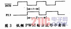
The specific control duty cycle process is as follows: After the MCU enters the external interrupt, P2.3 is set to a high level, delay for a period of time t, and then P2.3 is set to a low level. Thus, the P2.3 port outputs a rectangular wave with a duty ratio of q%=t/T. By changing the delay t, the duty ratio can be changed. The delay function is as follows: 
When the crystal oscillator of the MCU is 12 MHz, this function is delayed by 8c μs. It is assumed that the square wave with the output frequency of the AD9851 is sent to INT0. For example, if a rectangular wave with a duty ratio of q% is required, the following relationship is satisfied: 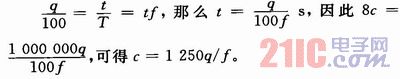
Therefore, when the delay time t=delay (1 250q/f), a rectangular wave with a frequency of f and a duty ratio of q% can be output from the P2.3 port. It should be noted that if the frequency is very high, T is small, because the delay function t is delayed by an integer multiple of 8 μs, so the accuracy of the duty cycle control cannot be guaranteed, and the higher the frequency, the lower the accuracy. Since the low frequency range of this design is in the range of 0 to 200 Hz, the square wave period sent by the AD9851 to the external interrupt pin is relatively large. Therefore, the above method can be used to control q to change within 0 to 100 accurately, and the output frequency is ideal. A low frequency PWM signal with independently adjustable duty cycle.
2.2 High-band PWM signal generation circuit SG3525 is a single-chip integrated pulse width modulation controller with excellent performance, complete functions and versatility. It is simple, reliable, easy to use and flexible, greatly simplifying the design and debugging of the control circuit. . Therefore, SG3525 is selected as the high-frequency PWM signal generator of this design to generate PWM signal of 200~25 000 Hz.
The high-band PWM signal generation circuit is shown in Figure 4. The MCU generates two analog voltage signals after two D/A conversions, which are used to control the duty cycle and frequency of the SG3525. By controlling the base voltage Ub of the FM three-stage tube Q1 to adjust the current on the 2-pin Non of the SG3525, the purpose of controlling the output PWM frequency of the SG3525 is achieved. By changing the base voltage Ub of the control three-stage tube Q2 to adjust the current on the 6-pin RT of the SG3525, the purpose of controlling the output duty cycle of the SG3525 is achieved. In this design, the 11-pin, 14-pin and 12-pin of the SG3525 are grounded, so that the PWM pulse is output by the 13-pin VC. This ensures that the output of the 13-pin is consistent with the output of the latch, and the output frequency duty cycle is independent. Adjust the PWM signal. In addition, since the output frequency and duty cycle are linear with the two analog voltage signals that control them, the software implementation is also very convenient. 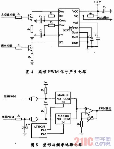
3 Frequency selection circuit It is necessary to combine the low frequency band and the high frequency band PWM signal to obtain the complete frequency segment PWM signal. Therefore, the frequency selection is required. The frequency selection circuit of the system is shown in FIG. 5 . First, the two PWM signals are respectively converted to the standard TTL level. The low-band PWM signal can achieve the TTL level through the 74LS00 and the pull-up resistor. In the high frequency band, the output amplitude of the SG3525 is 12 V, so the 5 V regulator is required. Decrease the amplitude and output the TTL level by the 74LS00 and pull-up resistors. The frequency is selected by the single-chip integrated analog switch MAX318. Here, the normally open pin NO is used as the input of the switch, and the common terminal COM is used as the output signal. The switch state is switched by the true value of the IN pin, which is controlled by the MCU I/O ports P2.3 and P2.4 respectively. When the IN logic true value is 0, the NO terminal is turned off. When the logic true value is 1, the guide is Pass N0 end. At the same time, only one chip's IN pin is high, and the other must be low. Otherwise, the two signals will crosstalk.
4 Optocoupler isolation and drive circuit The PWM control circuit and the drive circuit need to be electrically isolated to eliminate the interference of the main circuit to the signal generation circuit. The PWM signal current generated by the PWM signal generation circuit is too small to directly drive the power amplifier tube, and the amplitude of the output PWM power supply cannot be adjusted. Thus, the optocoupler isolation and drive circuit is designed. The circuit is shown in Figure 6. PWM is used as the control signal of the whole circuit. After the optocoupler is isolated and amplified, the two-stage switch transistor is used to control the on/off of the main circuit, and the PWM pulse with variable frequency and duty cycle is generated on the solenoid valve. The signal, at the same time, the MCU generates a variable analog voltage signal through D/A conversion. The signal passes through a voltage negative feedback circuit to stabilize the output voltage amplitude, and then increases the input current to drive the power tube through successive stages of the emitter follower. By changing the input voltage, the amplitude of the PWM voltage applied to the solenoid valve can be changed to achieve an arbitrary setting between 0 and 36 V. 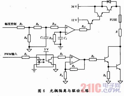
5 Conclusion Designed to simulate the working state of the automotive solenoid valve PWM power supply, through the matrix keyboard and LCD to achieve man-machine dialogue, through the microcontroller processing data to control the frequency, duty cycle and amplitude of the PWM wave, all data required for power supply It can be transmitted to the MCU through the keyboard and displayed in real time through the LCD. The control signal generated by the single-chip microcomputer simulates the actual working state of the electromagnetic valve, and can detect the quality requirements of the electromagnetic valve of the automobile under various working conditions, and ensure the quality of the electromagnetic valve before leaving the factory. The power supply is stable in operation and high in precision. It has been successfully applied to the production of automotive solenoid valves, which has created significant economic benefits for the enterprise and contributed to the export of solenoid valves in China.
This article refers to the address: http://
Stadium Light Bulbs are suitable for outdoor lighting, gardens, squares, billboards, factories, docks, stadiums and other places where lighting is needed.Stadium Light Bulbs have anti glare measures, and lamps and accessoriesmeet the environmental requirements.Led Stadium Light for stadium of high strength, corrosion resistance, and electrical accessories to meet the requirements of heat resistance.Creating a more sustainable sports stadium becomes that much more possible with Led Stadium Flood Lighting.With energy savings up to 75%, you can reduce a tremendous amount of energy consumption.With an increase in light quality and output, visibility becomes better. This creates better safety in two ways: for the players and the visitors.By enabling players to see better on the field or court, they will better be able to avoid potential accidents with Stadium Floodlights.In the same way, fans and visitors can feel safer in the stadium or in the parking lot with well-lit areas.
Stadium Light Bulbs
Led Stadium Light,Led Stadium Flood Lighting,Stadium Light Bulbs,Stadium Floodlights
Shenzhen Bbier Lighting Co., Ltd , http://www.chinabbier.com