Abstract: Aiming at the complexity of the locomotive high-power DC converter, it is easy to fault, and a relatively simple and reliable medium and high power DC converter is designed. The working principle of the DC converter of the multi-output locomotive is introduced. The new design method of the main circuit and the protection circuit is expounded. The problems that are easy to occur in the debugging are analyzed and the solution is given. The practical application shows that the DC converter has reliable operation and high efficiency, and has good practical value and promotion significance.
This article refers to the address: http://
Keywords: practical; multiple output; DC converter; protection circuit
 
1 Introduction
With the advancement of technology, it has become an inevitable trend to update the electronic equipment used in early diesel locomotives. The power supply on the diesel locomotive is generally provided by the generators it carries. In order to convert the output voltage of the generator into locomotive lighting, wireless dispatching and other electrical voltages, it must pass through a conversion device, the DC converter. At present, the multi-output DC converter commonly used on locomotives adopts self-excited push-pull and multi-stage conversion circuits. The structure is very complicated, and the phenomenon of "straight through" of the power tube is very easy to occur, and the converter can be slightly inadvertently used. Failure, causing unnecessary trouble or even safety hazards to the operation of the locomotive. To this end, this article will explore the design of multi-output DC converters with his push-pull circuit. The design does not use the conventional design method, but everything is simple and practical, and the protection circuit is very reliable design - Designed from multiple points on the original side. The practical application shows that the converter has simple structure, reliable operation, high efficiency and strong practicability.
2 Introduction of multi-output locomotive DC converter
The DC converter has an input voltage range of 70 to 135V (rated at 110V) and an output of 24V, 50V, etc. The output rated current is 4A. It can be seen that the output power is about: P = (24 + 50) 4 = 296W, which is a medium-high power converter. It is difficult to provide such a large current directly with a forward or flyback circuit, considering the use of a half bridge and a full bridge circuit. Relatively complex, he used his push-pull circuit. The main circuit includes input filter circuit, output filter circuit, auxiliary power supply circuit, control circuit, drive circuit, feedback detection circuit, power conversion circuit, protection circuit, etc. The circuit structure diagram is shown in Figure 1.
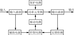
Figure 1 overall circuit structure
The working principle of the converter is as follows: The pulse width modulator constituting the control circuit can generate a driving signal with a fixed frequency and a pulse width adjustable, and control two power tubes S 1 and S 2 (as shown in FIG. 3 ) with a phase difference of 180°. Alternate switching to adjust the output voltage level, using the error amplifier and the voltage measuring comparator to form a voltage closed loop through the optocoupler, the output voltage is divided by the precision resistor and then compared with the reference voltage, thereby adjusting the duty cycle of the driving signal to make the output voltage It changes with the change of the error voltage. If the output voltage rises for some reason (such as input change, load change, etc.), the pulse width modulator changes the pulse width of the drive signal, that is, the duty ratio D , so that after the chopping The average voltage drops to achieve regulation and vice versa. For the input rise, the voltage regulation process is shown in Figure 2.
![]()
Figure 2 Output voltage regulation diagram
The main circuit of the DC converter and the protection circuit are used to clarify the design idea of ​​the converter and discuss various problems that are easy to occur in debugging.
3 DC converter main circuit design
In the main circuit is the use of his push-pull circuit, as shown in Figure 3.
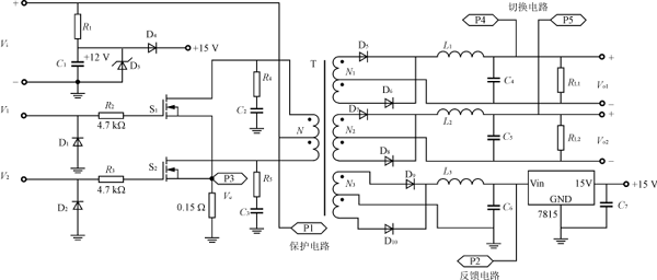
Figure 3 main circuit diagram
In Figure 3, V i is the filtered input voltage. V 1 and V 2 are drive signals that are 180° out of phase with each other from the pulse width modulator. P 1 and P 3 are used to design the protection circuit, and P 2 is used to design the feedback detection circuit. P 4 and P 5 are used to design the switching circuit. In the figure, the power tube can withstand twice the input voltage, that is, the maximum voltage is 270V, and the current does not exceed 4A at most. Therefore, the power tube can be used with IRF460. N 3 third transformer output voltage to provide power to the control circuit by design. At the beginning of power-on, the output of N 3 is 0. The control circuit power supply voltage is provided by the input voltage divider and voltage regulation (composed of R 1 , C 1 , D 3 ). When the circuit works normally, D 4 is cut off, control circuit and protection. supply voltage circuit or the like through output 7815 N 3 by the voltage regulator.
The transformer is the most important part of the switching power supply. The conventional design is derived using a large number of complicated formulas. Due to the large amount of calculation, it is inevitable that the result will be wrong. In view of this, this paper uses the method of chart to design the original and secondary sides, and considers the actual conditions such as the tube conduction voltage drop to make appropriate fine adjustment. Since the primary and secondary currents of the converter are both large, a multi-strand wire is used. The specific design of the double-ended forward circuit is as follows.
n 1 d p 2 = ![]() n 2 d s 2 =
n 2 d s 2 = ![]() ;
;
Where: n 1 , n 2 are the number of strands of the primary and secondary windings;
d p , d s is the wire diameter of the primary and secondary windings;
S o K o is the area of ​​the core window used;
N p , N s is the number of turns of the primary and secondary windings.
Where: N p = ![]() ; N s =
; N s = ![]()
U i is the input DC voltage;
U 1T is the voltage value per turn;
U V is the rectifier pressure drop;
D is the duty ratio, which is 0.6 for the double-ended circuit D.
The working frequency of the transformer is 100 kHz, so the wire diameter can be selected as 0.5 mm. The core of the transformer is EI-type ferrite EI-50, check EI-50
The attribute comparison chart shows that the window use area is 48.97 mm 2 and the voltage value per turn is 8.044 V/åŒ. This can be obtained: the original side, the stock
The number is 12åŒ, 8 shares; the secondary side, the number of shares is 11åŒ, 5 shares/6åŒ, 5 shares. In actual debugging, converter working time
For a long time, the core temperature will increase slightly, and the output voltage ratio will be somewhat out of tune. After many fine adjustments, the original and secondary sides will be counted.
Set at 12 åŒ, 10 åŒ / 5 åŒ, in this case, the transformer temperature does not rise, the output voltage is also consistent with the expected value.
A special consideration for the use of push-pull circuits is the problem of flux saturation. This is due to the unbalanced turn-on and turn-off time of the two power transistors. Over time, it will cause bias. In addition, when one tube is turned off and another tube is turned on, a spike will appear. The solution can be added to the main circuit plus the absorption circuit, as shown in Figure 3 R 4 and C 2 and R 5 and C 3 . If the output is a composite filter (capacitor-inductive filtering), it can be considered to eliminate the spikes by stringing a resistor with a small resistance value on the output capacitor.
For two power tubes in the main circuit, due to alternate conduction, when one tube is turned on under the positive pulse of the gate, the other tube has lost the gate forward drive signal, but due to the storage time, The second tube is not immediately cut off, but is still in the on state, resulting in a "straight through" phenomenon in which two power tubes are simultaneously turned on. Although the time is short, it is very harmful to the circuit. This phenomenon can be eliminated by shortening the storage time of the power-off tube, preventing the power tube from entering deep saturation and preventing excessive excitation of the tube. A clamping diode can be used in the design to avoid the transistor from entering deep saturation. Its circuit is shown as D1 and D2 in Figure 3. Once the power transistor enters the saturation region, the clamp diode shunts the gate's excitation current to the drain so that the gate current does not increase, thus preventing the power transistor from entering deep saturation, thereby reducing storage time.
In the output filter design, in order to ensure that several output voltages change in proportion, try to make the ratio of inductance to capacitance larger. Of course, a balanced circuit can also be designed to solve this problem.
4 DC converter protection circuit design
The locomotive DC converter is related to the safety problem of locomotives. In order to improve the quality of power consumption and effectively protect the DC converter, it is especially important to design a good protection circuit. Since the converter input voltage designed in this paper has a range, overvoltage and undervoltage protection must be considered. Overcurrent protection must also be considered in the event of a circuit failure that causes the current to rise.
The control chip of the DC converter uses TL494, which is a voltage-driven pulse width modulation control integrated circuit produced by Texas Instruments. It is a well-designed protection circuit and its resource condition is very clear. The internal circuit of the TL494 consists of a reference voltage generation circuit, an oscillation circuit, an intermittent period adjustment circuit, two error amplifiers, a pulse width modulation comparator, and an output circuit. Figure 4 is a diagram of its pin, where pin 1 and pin 2 are the in-phase and inverting inputs of error amplifier I; pin 3 is phase correction and gain control; and pin 4 is intermittent, which is 0-3.3V applied When the voltage is applied, the cut-off time can be linearly changed from 2% to 100%; the feet 5 and 6 are used for the external oscillating resistor and the oscillating capacitor respectively; the foot 7 is the grounding terminal; the foot 8 pin 9 and the foot 10 pin 11 are respectively the TL494 internal two The final output triode collector and emitter; the pin 12 is the power supply terminal; the pin 13 is the output control terminal, the pin is grounded for the parallel single-ended output mode, the pin 14 is the push-pull output mode; the pin 14 is the 5V The reference voltage output terminal has a maximum output current of 10 mA; pins 15 and 16 are the inverting and non-inverting input terminals of the error amplifier II. Since the error amplifier I has been designed for the feedback circuit to make the output constant, the protection circuit must be designed with the error amplifier II of the TL494, which uses underpin 15, overvoltage and overcurrent protection with pins 15 and 16. In order to ensure that the protection circuit can play a good protection when the input voltage exceeds the design range, the DC converter selects the protection circuit at multiple points on the primary side. It turns out that this effect is very ideal, as shown in Figure 5.
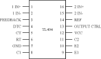
Figure 4 TL494 pin diagram
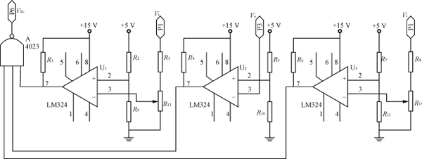
Figure 5 Schematic diagram of the protection circuit
In Figure 5, comparators U 1 and U 3 are used to design overvoltage and undervoltage protection, so voltage acquisition is important. In the past, it was always designed on the secondary side of the transformer. In fact, after passing through the transformer, the secondary side has a certain lag with respect to the primary side. Therefore, it is more reasonable to design the primary side and the undervoltage. Since the input voltage range is from 75 to 135V, the peripheral resistance can be estimated reasonably by two critical points of 75V and 135V to determine the resistance.
Comparator U 2 is used to design overcurrent protection. A small 0.15Ω resistor is used on the source string of the two switches to obtain the voltage value of the overcurrent detection (see V e of Figure 3 of the main circuit). The input current is calculated at a maximum of 4A. When the circuit is operating, the power transistor is turned on, and the current flowing through the drain and source is equal. For the 0.15V small resistor in Figure 3, the ground voltage is V e = 0.15 × 4 = 0.6V, so the appropriate resistor ratio can be selected to design the LM234's non-inverting terminal voltage to be about 0.6V.
Because there is no two levels of 0 or 1 output from the comparator, regardless of overvoltage, undervoltage, or overcurrent, a NAND gate is introduced, and its output V II- is connected to the inverting terminal of the TL494 comparator II (pin 15). ), any of the above conditions will cause the NAND gate to output a low level, thus causing the TL494 to turn off and the circuit to stop working.
In addition, a relay-based switching circuit must be designed at the output end. When the output of the inverter fails to provide an output voltage, the relay operates to switch the power on the locomotive to the backup battery to ensure the continuity of the locomotive power supply.
5 related experimental waveforms
The two power tube gate drive signals and the transformer primary side waveforms are shown in Figures 6 and 7, respectively.
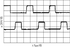
Figure 6 Power tube gate drive signal waveform
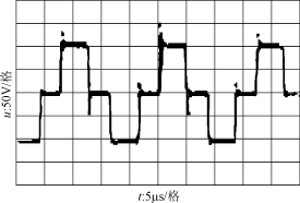
Figure 7 Transformer primary side waveform
6 Conclusion
For the medium and high power converters that cannot directly apply the forward or flyback circuit design, and at the same time, the bridge circuit design is relatively complicated, this paper provides a main circuit with his push-pull circuit. Relatively simple and practical design method, in addition, after the main circuit design is completed, how to design the subsequent circuit is often overlooked. This paper has carried out a more detailed exploration of this aspect. The multi-output DC converter has been running on the trains of Nanchang Railway Bureau and Shandong Railway Bureau for one year, and the effect is good.
Knonew
About KNONEW Lighting, focuses on creating the best lighting experience. Only high end LED and advanced optical design are adopted. Enjoy lighting with KNONEW.
KNONEW focuses on selling Led Curtain Lights in the USA
Our products have passed UL588, IP44 certification
Tested before delivery
And were Confirmed as qualified products
led curtain lights
led curtain
Specifications:
Color :Warm White
Color Temperature: Warm White 3000K
Input Voltage of Adaptor: 120V
Input Voltage of String Light: DC 30V
LEDs Quantity: 300
Lifespan: 50000hrs
Interval btw strings: 0.18m (7in)
Size: 3M (9.84ft) x 2M (6.56ft);
Material: Plastic+Copper;
Plug wire to the controller: 1.5m/4.9ft
If you have any questions about our product, please tell us, we will do our best to solved it for you!!!
The LED Curtain Lights : Led String Lights Widely Used Christmas trees,party, wedding, home, window, bathroom, festival, Holiday, shows, restaurant, hotel, commercial building, shopping center, shopcase, pub, club,concert, hall, cabaret, fashion show, dance, stage, etc.
Led Curtain Lights,Warm White Curtain Lights,Outdoor Led Curtain Lights,White Led Curtain Lights
Dongguan Xingyong Indusrtial Co,Ltd , http://www.xingyongled.com