With the rapid development of the IT industry and communication technology, electronic technology, and computer technology, a large number of production equipment and products are becoming more and more electronic, digital, automated, and intelligent. The electronic measuring equipment must be adapted to this. Kind of situation. Therefore, the integrated test technology, electronic technology, automation technology and computer technology integrated automatic test system development is increasingly perfect, in some highly electronic products, aerospace and military weapons and equipment, as well as industrial automation, communications, optics, energy and many other fields. It has been widely used.
The general meaning of the automatic test system refers to a system that uses computer control to achieve automated testing. Such systems are usually built on the basis of standard measurement and control buses or instrument buses (CAMAC, GPIB, VXI, PXI, CAN, etc.). At present, the Universal Serial Bus (USB) has become a widely used peripheral connection specification in the PC field due to its convenient plug-and-play and hot-swap characteristics and high transmission rate. The automatic test and diagnosis system introduced in this paper is based on five P89C668 single-chip microcomputers as the core fault diagnosis platform. The communication card based on FT245BM USB chip is used to establish a bridge between computer and test and diagnostic platform communication, so that it can be used for the combined logic digital circuit board that needs to be tested. Tests are performed and automatic fault location can be performed on the faulty board based on the standard diagnostics database. The system is currently capable of automated testing and troubleshooting of a variety of digital boards that do not contain uncontrolled components such as CPUs, memory components, crystals, resistive-capacitance monostable, etc. The maximum board edge connectors that can be tested The number of pins is 96.
1 hardware structureThe hardware of the test diagnostic system is mainly composed of the following parts:
·computer
·USB communication cable
·USB communication card
·Multiple MCU system test and diagnosis platform
·Micro switching power supply
·The cooling fan
·Channel connection adapter board, etc.
1.1 computer
The main function of the computer is to control the test and diagnosis platform through the USB interface, and then complete the test platform system self-test, channel input/output definition, send test stimulus data, receive response data, data calculation and analysis.
1.2 USB communication card
The USB communication card is a bridge between the computer and the test platform. Its main function is to send the control commands and data sent by the computer to the main MCU of the test platform, so that the test platform can complete various test tasks; on the other hand, it will test the self-test information and test results of multiple MCU systems in the test platform. Sent to the computer for computer judgment and analysis.
The USB communication card is based on FTDI's FT8U245BM chip and has the advantages of high data transfer rate (up to 8Mb/s) and plug-and-play.
1.3 Test platform composed of multiple MCU systems
A multi-MCU system consists of one master MCU and four slave MCUs. All MCUs use PHILIPS' P89C668 microcontroller chip, which has 64KB Flash program memory and 8KB RAM for ISP/IAP programming. It can take six clock cycles per machine cycle, which is twice that of traditional single-chip microcomputer (80C51). It has framing error detection and automatic address recognition in its full-duplex enhanced UART. It also has a programmable clock output function and a programmable counter array (PCA). It is a relatively high-end product in the PHILIPS MCU family. The test platform composed of multiple MCU systems is shown in Figure 1.
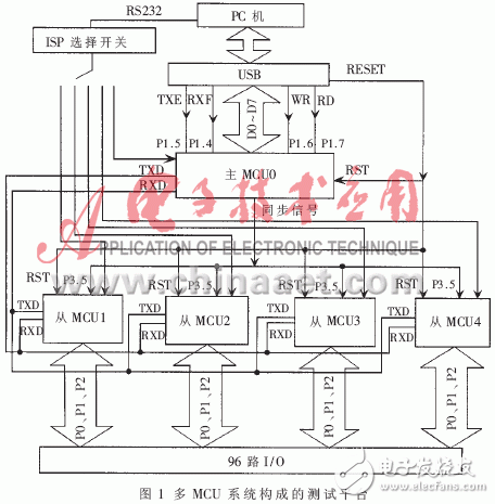
In the multi-MCU system designed in this paper, the functions of each MCU are as follows:
(1) Function of the host MCU
· Responsible for communication with the PC. Communication adopts the popular USB bus communication method, which receives commands and data from the PC on the one hand, and sends test data and self-test information to the PC on the other hand.
• Interpret commands from the PC and send them to all slaves or the corresponding slaves. The data from the PC is sorted and sent to the corresponding slave. Perform a self-test on its own RAM.
· Responsible for communication with four slaves. The communication is multi-master master-slave mode, using the RxD and TxD terminals of the MCU to communicate in full-duplex UART serial mode, and using frame error detection and automatic address recognition.
· Manage four slaves for simultaneous testing. The main MCU uses the lower four bits (P1.4, P1.5, P1.6, P1.7) of the P1 port to send synchronization control signals to the four slaves, so that multiple slaves can maintain synchronization during the test.
(2) Functions of slave MCU1 to MCU4
• Receives commands and data related to itself from the host MCU via serial communication via the RxD port.
• A total of 96 channels of each of the 24 I/O ports P0.0 to P0.7, P1.0 to P1.7, and P2.0 to P2.7 of each slave are connected to test channels Port1 to Port96. According to the setting of the I/O port, the test excitation signal is output to the defined output channel, and the test result is read from the corresponding input channel and stored in the corresponding RAM unit.
• After testing an output channel of the tested board, send the test result to the RAM memory area of ​​the main MCU and send it to the computer by the main MCU.
· Responsible for the self-test of RAM in its own data storage area. When receiving the self-test command of the main MCU, it performs a self-test on its own RAM and sends the self-test result to the main MCU.
1.4 Test Channel Adaptation Interface Card
Ordinary digital boards to be tested cannot be directly plugged into the test interface of the test platform. A special test channel adapter interface card is required to connect. The interface card provided by this system is a 96-channel bus structure interface card, which can be connected with the digital circuit board suitable for this design. If you want to test other types of digital boards, you need to customize the test channel adapter interface card.
2 software design2.1 Test Platform Programming
The system test platform program adopts modular design and is based on Keil system development software and TKS-668 development hardware, which is written in C language and assembly language. The idea of ​​modular programming is to divide a complex program into a number of relatively independent program modules according to the overall function. Each module can be individually designed, programmed, debugged and debugged, and then assembled for joint debugging, eventually becoming a practical one. The process of value. The test platform software of this system is mainly composed of the main program of the system, the communication program, the test program and the self-test program.
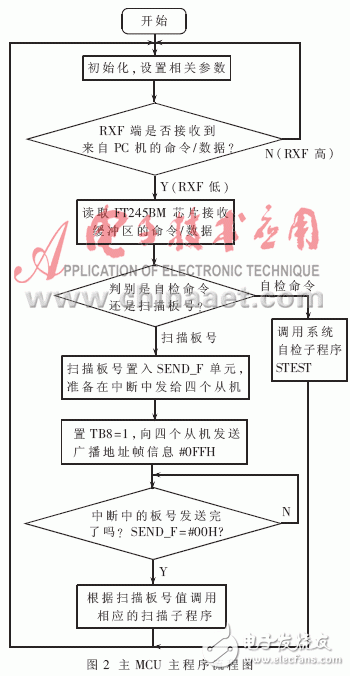
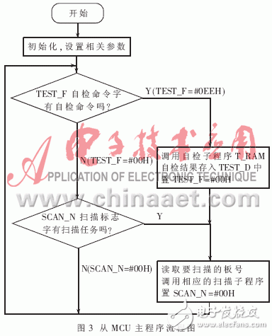
2.1.1 main program design
The main program design flow diagrams of the master and slave MCUs are shown in Figure 2 and Figure 3, respectively. The four slave MCUs in this system have the same function, so the main program design is the same. The relevant parameters to be set by the master and slave MCU during initialization include: serial port mode, baud rate, timer mode, and interrupt.
2.1.2 Self-test program design
The master-slave MCU self-test is to ensure that each MCU can work normally, that is, the communication between the USB and the main MCU, the main MCU and the slave MCU is normal, and the RAM of each MCU is not damaged.
Whether the communication between the main MCU and the slave MCU is normal is: first, the main MCU sends a string of data to the slave MCU, and then the data received from the MCU is sent back to the main MCU to determine the number of two strings of data. Whether the content is consistent or not, the communication is normal. Similarly, the principle of communication self-test between USB and main MCU is also the same.
The principle of the MCU's RAM self-test is: for each RAM memory cell, first write a data to the RAM cell, and then read a data from the cell to determine whether the two are consistent. The RAM unit is not damaged.
2.1.3 Communication program design
The communication program of the system includes: a communication program between the main MCU and the USB, a communication program between the main MCU and the slave MCU, and a scanning program from the MCU to the detected circuit board.
The main MCU and USB transfer data through the pins D0~D7 of the USB and the pins P0.0~P0.7 of the main MCU. Control is mainly carried out through four pins of USB: RXF, TXE, WR, /RD and four pins of the main MCU: P1.4, P1.5, P1.6, P1.7. When TXE is low and WR changes from 0 to 1, data is written to USB; when RXF is low and /RD changes from 1 to 0, data is read from the USB to the primary MCU. The main MCU judges the RXF and TXE of the USB through P1.4 and P1.5, and then transfers data to the WR and /RD of the USB through P1.6 and P1.7.
The main MCU and the slave MCU use the RxD and TxD terminals of the MCU to communicate in the full-duplex UART serial mode. The serial communication is realized by interrupt, and the frame error detection and automatic address recognition functions are used. The main MCU of the system adopts the broadcast communication mode, and the special register SADEN and SADDR logic or generate the slave's broadcast address, and use the address automatic identification function to send a broadcast address and simultaneously send commands to communicate with four slave MCUs. When the main MCU only communicates with a single slave MCU, the dot-point communication method is adopted, and the specific addresses generated by SADEN and SADDR are used to confirm which slaves are selected to communicate with the host, and no software query is required.
The function test technique is used from the MCU to scan the board to be tested. In order to detect the fault of a certain combination logic board, first insert the board into the diagnostic socket. Since each output port is only logically related to several of the ports of the board, the scanning program only needs to The input port of the board that is logically related to an output port is level-inspired from all 0s to all 1s (for example, there are five input ports, a total of 25 = 32 sets of excitation). When there are more than seven inputs with logical relationship, since the workload is very large, the excitation from all 0s to all 1s is not performed, but 128 sets of excitations are selected to perform similar sampling detection, and then the output port is read and the output is output. The results are transmitted to the computer, and the simulation results in the standard database are analyzed and compared to determine whether they are consistent. If there is an inconsistency, the board is faulty.
2.2 Application System Software DesignThe automatic test diagnostic system software installed on the computer is programmed in Visual C 6.0 language. Its main function is to enable the computer to send test stimulus data, receive response data, perform data calculation and analysis to the USB interface communication card.
2.3 Software generation method for standard diagnostic databaseThe purpose of establishing a standard diagnostic database is for automatic fault location. The system can establish a standard diagnostic database in two ways: The first method is to generate a standard diagnostic database through simulation functions in some EDA software environments such as Protel, FoudaTIon, and Maxplus II according to the schematic diagram of the digital board under test. The second is to test the function of the digital circuit board, record the response data of the board under a specific excitation, automatically added to the corresponding database by the software, as a standard diagnostic database to test the board in the future.
Since the number of circuit board ports to be tested and diagnosed by this system is large, the second method is not only a very large workload, but also ensures that the digital circuit board under test is functioning normally during the test, so the system adopts the first method. Considering that the measured circuit board is a combined logic digital circuit board, the system uses the FoundinTIon F3.1i software environment of Xilinx, inputs the schematic of the digital circuit board under test in the SchemaTIc Editor, and then The Script Editor of the Function Simulator (FuncTIonal Simulation) automatically generates standard diagnostic data files using the simulation commands provided by the software, and then the application system software imports the data into the corresponding database.
At present, the general automatic test and diagnosis system is usually formed on the basis of a standard measurement and control bus or instrument bus (CAMAC, GPIB, VXI, PXI, CAN, etc.), which is costly, bulky, and complicated to operate. It is very inconvenient in the process and it is difficult to meet the needs of modern science and technology workers. The automatic test and diagnosis system introduced in this paper is based on five P89C668 single-chip microcomputers as the core fault diagnosis platform. The communication card based on FT245BM USB chip is used to realize the communication between the computer and the test and diagnosis platform. The portable structure of the system is particularly suitable for field testing, and has the advantages of low cost, small size, light weight, compact structure, high degree of automation, etc. The operation of the system is relatively simple, as long as the general operation of the computer is mastered, it has a certain digital circuit technology foundation. Can understand the general digital circuit schematic, after a simple technical training, read and understand the operating instructions of the system can be operated; the standardization of the system hardware module and the reusability of the software module make the system very strong Expansion ability. At present, the test and diagnosis system has been put into use, and the effect is good, which fully achieves the intended design goal.
Fiber Optic Patch Panel,Fiber Patch Panel,Fiber Distribution Panel,Optical Patch Panel
Cixi Dani Plastic Products Co.,Ltd , https://www.dani-fiber-optic.com