I. Introduction
The Sis-based Mosfet tube has a high input impedance, a small driving power, a simple driving circuit, and a working characteristic of majority carriers, and has no storage time required for a minority carrier to work, and thus has a fast switching speed. The operating frequency can be up to 500kHz or even more than MHz. However, as its reverse withstand voltage increases, the on-state resistance also rises sharply, which limits its application in high-voltage applications. IGBTs have high reverse voltage and high current characteristics, but they are very strict on the drive circuit and are not suitable for high frequency applications. Generally, IGBTs operate at frequencies below 20 kHz.
As a wide-forbidden semiconductor device, SiC has high saturation electron drift velocity, high electric field breakdown strength, low dielectric constant and high thermal conductivity. The SiC-based Mosfet tube has the characteristics of high blocking voltage, high operating frequency and high temperature resistance, low on-state resistance and low switching loss. It is an application of high power density and efficiency improvement in high frequency and high voltage applications. trend.
Second, SiC Mosfet and Si IGBT performance comparison
At present, the common SiC Mosfet currents on the market are no more than 50A. Taking the common 1200V/20A as an example, some electrical parameters of Cree and Rohm's SiC Mosfet tubes are listed. The Fairchild and APT 1200V/20A are also exemplified. Comparison of electrical parameters of the Si IGBT series;
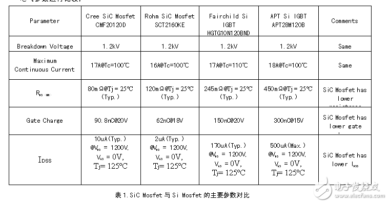
Table 1. Comparison of main parameters of SiC Mosfet and Si Mosfet
Through the comparison of the table performance, it can be seen that the performance of SiC Mosfet has three aspects is significantly better than Si IGBT:
1. Extremely low on-resistance RDS(ON) results in extremely superior forward voltage drop and conduction loss, and is more suitable for operation in high temperature environments;
2. The SiC Mosfet tube has the input characteristics of the Si Mosfet tube, ie a relatively low gate charge, resulting in an excellent switching rate of performance;
3. Wide band gap material with relatively low leakage current, which is more suitable for high voltage environment applications;
Third, the drive circuit requirements
Sic Mosfet has very similar switching characteristics to Si Mosfet tubes. By studying the characteristics of Si Mosfet, its driving circuit has the same characteristics:
1. For the driver circuit, the most important parameter is the gate charge. The gate input of the Mosfet tube is equivalent to a capacitive network, so the device does not need to drive current during the stable on-time or off-off time. However, during the switching process of the device, the input capacitance of the gate needs to be charged and discharged, and the gate driving circuit must provide a sufficiently large charge and discharge pulse current. If the operating frequency of the device is faster, the shorter the charge and discharge time requirement of the gate capacitor is, the smaller the gate capacitance of the input is required, and the larger the pulse current of the driving is to satisfy the driving requirement;
2. The gate drive circuit must reasonably select a certain driving voltage. The higher the driving voltage of the gate, the larger the inductive conduction channel of Mosfet is, the smaller the on-resistance is. However, if the gate driving voltage is too large, it is easy. Breaking down the insulating layer between the gate and the drain, causing permanent failure of the Mosfet tube;
3. In order to increase the speed of the switching tube, it is necessary to reduce the off time of the switching tube; and in order to improve the reliability of the Mosfet tube in the off state, the driving circuit is designed to be in the off state, in the gate Extremely reverse bias voltage to quickly release the charge of the gate input capacitor, reducing the turn-off time, making the drive circuit more reliably turn off the Mosfet; but the reverse drive voltage increases circuit losses, reverse bias The voltage should preferably not exceed -6V;
4. When the driving object is the power Mosfet of the full bridge or half bridge circuit, or to improve the anti-interference ability of the control circuit, the driving circuit is designed as an isolated driving circuit at this time; the way of electrically isolating can be through the magnetic coupling transformer and the optical coupling The device; however, whether using a magnetically coupled transformer or an optically coupled device, the delay time of the coupled device and the coupled distributed capacitance are guaranteed; the isolated power supply must also have high isolation, fast response time, and low coupling capacitance.
Fourth, isolated power supply characteristics needs
From the characteristics of the drive circuit, the drive power supply is required to have the following characteristics:
1. In order to meet the requirements of high frequency use, the driving power source is required to have instantaneous driving high power characteristics, that is, it requires a large capacitive load capacity;
2. In order to meet the requirements of high voltage applications, the drive power supply is required to have high withstand voltage capability and has an ultra-low isolation capacitance to reduce the interference of the high voltage bus part on the low voltage control side;
3. The isolated drive power supply must have a suitable drive voltage, that is, the power supply is required to have positive and negative output voltages, and the positive and negative output voltages are not symmetric output characteristics;

Jin Shengyang has introduced the SiC Mosfet drive dedicated power supply QA01C for the characteristics of the SiC isolation drive circuit. The electrical performance parameters of the power supply all meet the requirements of the SiC Mosfet drive circuit, such as:
?Asymmetric drive voltage, output voltage +20/-4VDC output current +100/-100mA
Large capacitive load capacity with a capacitive load of 220uF
High isolation voltage up to 3500VAC
Very low isolation capacitance down to 3.5pF
This drive power also meets the characteristics of other performance parameters, the specific functions are as follows:
? Efficiency up to 83%
? Operating temperature range: -40°C ~ +105°C
? Sustainable short circuit protection
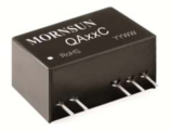
Figure 1. QA01C physical map
The QA01C has a complete driver circuit recommendation. The SiC drive dedicated power supply provides an asymmetric forward drive voltage of 20V and a negative bias turn-off voltage of -4V. To prevent damage to the gate caused by the drive voltage, increase D2 and D3 to absorb spikes. Voltage is necessary. The SiC driver can be driven by a general driver chip; in order to isolate the control signal from the main power loop, isolation measures are required. A common optocoupler isolation scheme is recommended. The optocoupler used must have a high common-mode rejection ratio (30KV/us) and a large isolation withstand voltage compared to an isolated power supply with minimal delay time to accommodate the high frequency operating characteristics of SiC Mosfet tubes.
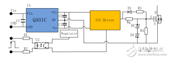
Figure 2. SiC driver circuit recommendation
V. Summary
By comparing the electrical parameters of SiC Mosfet tube with Si IGBT tube, we found that SiC Mosfet will become the application trend in high voltage and high frequency applications. According to the research on the switching characteristics of SiC Mosfet tube, Jin Shengyang recommended the special power supply QA01C which can simplify its isolation design, and also recommended the driving circuit based on SiC Mosfet.
references:
[1] Money lighting, etc. China Electrical Engineering Dictionary [M]. Beijing: China Electric Power Press, 2009.6
[2] Keith Billings. Zhang Zhansong and other translations. Switching Power Supply Manual [M]. Beijing: People's Posts and Telecommunications Press, 2006.12
[3] Tong Shi Baihua Cheng Ying. Analog Electronic Technology Foundation [M]. Beijing: Higher Education Press, 1999
Commercial electric LED emergency double heads light is perfect for applications requiring a dependable, long lasting, energy efficient life safety solution with a traditional design. The twin heads emergency light is designed with injection-molded, flame-retardant, high impact thermoplastic housing .The adjustable heads allow for optimal lighting of the path of egress.

Emergency Exit Lights,2 Head Emergency Light,Twin Spot Emergency Light,Led Twin Spot Emergency Lights
Jiangmen City Pengjiang District Qihui Lighting Electrical Appliances Co., Ltd , https://www.qihuilights.com