The shift register instruction SHRB shifts the DATA value into the shift register. S_BIT specifies the lowest bit of the shift register. N specifies the length of the shift register and the shift direction (shift plus = N, shift minus = -N). The maximum length of the shift register is 64 bits and can be either positive or negative. It should be noted that each bit shifted out by the SHRB instruction is placed in the overflow memory bit (SM1.1).
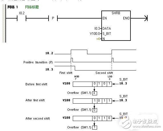
The following procedure is used to explain the use of the instruction. The shift register instruction is executed with the rising edge of I0.2. That is, one scan period is shifted by one bit. In the instruction, V100.0 is the lowest bit of the shift register, I0. The value stored in .3 is 0 or 1. The instruction specifies that the shift is added. The length of the shift register is 4. We combine the following timing diagram and shift diagram. If V100 is 0000 0101, since the length of the shift register is 4, then only 0101, when I0.3 is 1, the first shift is performed, and 1 is executed. Move to the lowest bit of the shift register, put the value 0 of the shifted bit into SM1.1, then SM1.1 is 0, when I0.3 is 0, perform the second shift, move 0 to shift The lowest bit of the bit register, put the value of the shifted bit into SM1.1, then SM1.1 is 1.
In sequential control or step control, it is convenient to apply shift register programming. The shift register instructions are as shown.
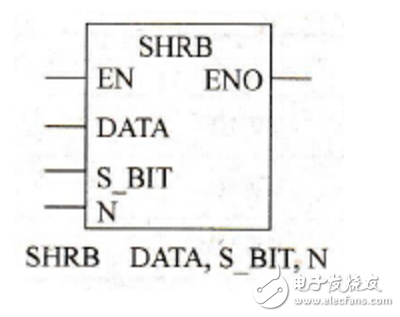
1) The shift register has 3 data inputs:
DATA: Data input of the shift register, the data type is BOOL (bit).
S_BIT: The lowest bit that makes up the shift register, the data type is BOOL (bit).
N: shift register length and shift direction, -64 ≤ N ≤ 64, when N "0" is forward shift (from the lowest shift of the shift register, from the highest displacement), when N "0" For the reverse shift (into the highest displacement of the shift register, the lowest displacement).
2) Features of the shift register:
The data type of the shift register is not divided into a byte type, a word type, or a double word type, and the length N of the shift register is specified by the program.
· The composition of the shift register:
The lowest bit is: S_BIT;
The highest-order calculation method is: MSB=S_BIT+(|N|-1)/8. The addressing of the S7-200 is octal. When adding, the byte and byte are added together, the bit and the bit are added, and every 8 is entered into 1; for example:
S_BIT= V23.4, N=15, then MSB= V23.4+(15-1)/8= ![]()
The composition of the shift register: V23.4~V23.7, V24.0~V24.7, V25.0, V25.1, V25.2, a total of 15 bits.
The function of the shift register instruction is: when the enable input EN is valid, if N "0, the shift data DATA is filled in the lowest bit of the shift register (S_BIT); if N "0, then fill in the shift The most significant bit of the bit register, the other bits of the shift register are serially shifted in the direction specified by N (forward or reverse).
• The shift register is connected to SM1.1 (overflow).
Special relays affected by shift register instructions: SM1.0 (zero), SM1.1 (overflow). When the shift operation result is 0, SM1.0 is automatically set; the state of SM1.1 is determined by the state of each shift bit.
The error conditions that affect the allowable output ENO to work properly are: SM4.3 (run time), 0006 (indirect addressing), 0091 (operand out of bounds), and 0092 (counting area error).
Inverter 12V,Inverter 4000W 12V,Portable Mini Inverter 12 V,Solar Power Inverter 12V
GuangZhou HanFong New Energy Technology Co. , Ltd. , https://www.gzinverter.com