Some embedded systems use multitasking for operation and control. These systems must provide a mechanism to ensure that running tasks do not disrupt the operation of other tasks. That is to prevent system resources and other tasks from being illegally accessed. Embedded systems have specialized hardware to detect and limit access to system resources. It guarantees the ownership of resources, tasks need to comply with a set of hardware-maintained rules defined by the operating environment, and grant special permissions to monitor and control resource programs at the hardware level. Protected systems proactively prevent one task from using resources from other tasks. Therefore, using hardware proactive monitoring systems provides better protection than coordinating enhanced software processes.
The Memory Protection Unit (MPU) is a type of hardware that is effectively protected by the ARM and provides memory area protection.
MPU register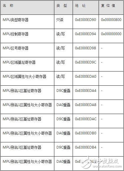
The coprocessor registers associated with the MPU are mainly c2, c3, c5 and c6. There are also 1 to 2 bits in register c1.
(1) MPU related bits in c1
The encoding format of c1 is as shown.
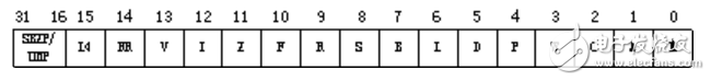
The M(bit[0]) control controls the enabling of the MPU.
· M=0: MPU is prohibited
· M=1: Enable MPU
A (bit[1]) selects whether to support memory access address alignment check.
· B=0: Disable address alignment check
· B=1: Enable address alignment check
(2) MPU related bits in c2
The encoding format of c2 is shown in the figure.
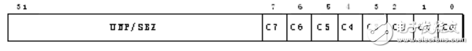
Register bits 0 to 7 correspond to the Cache attributes of fields 0 to 7, respectively. Bits 8 to 31 should be set to 0.
Note that in systems where data and instructions are separate, the D-Cache and I-Cache attributes are read and written by the second operand "opcode2" of the MRC and MCR instructions.
(3) MPU related bits in c3
The encoding format of c3 is shown in the figure.
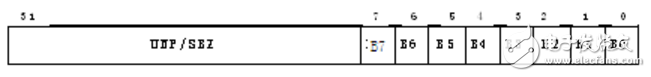
Register bits 0 to 7 correspond to the write cache attributes of fields 0 to 7, respectively. Bits 8 to 31 should be set to 0.
When reading and writing c3 with the MCR/MRC instruction, the second operand "opcode2" will be ignored and the instruction will be set to 0.
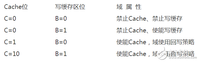
When configuring a data domain, the domain's cache bit and the write cache location together determine the domain's access policy. The write cache bit has two purposes: to enable/disable domain write caching and to set the domain's Cache write strategy. The Cache bit of the field controls the role of the write cache bit. The specific bit allocation is shown in the table below.
(4) Access permission register c5
The register c5 of the coprocessor CP15 sets the access rights of the memory domain.
The encoding format of register c5 is as shown.
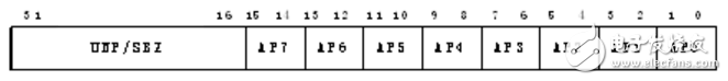
Read the bits[15:0] of register c3 to store the AP (access permission) of the domain, where bits[2n+1:2n] have access rights to domain n. The correspondence between AP coding and access rights is shown in the following table.

For the two kernel versions of Arm940T and Arm940T, when the MRC and MCR instructions are used to read and write, the second coprocessor register "CRm" will be ignored, and the instruction will appear as c0. For the field in which the instruction data is unified, the second operand "opcode2" is set to 0, and for systems with separate data and instructions, if opcode2=0, the operation is valid for the data field, and if opcode=1, the operation is for the instruction field. effective.
Note that for the two kernel versions of Arm946E-S and Arm1026EJ-S, their access rights are more complex, using extended APs, and the extended group AP bitfield encoding supports two enhanced permission domains, which operate on MRC and MCR. The form of the instruction is more complicated. For more detailed content, please participate in the user manual of Arm.
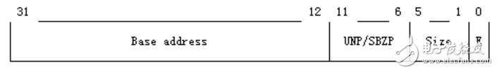
(5) Domain size control register c6
In the Arm system, the size of the domain is defined by the write coprocessor c6, and the second operation register in the MCR instruction assigns a different value to indicate which specific domain is to be operated. The second operation register takes values ​​from c0 to c7, corresponding to domain 0 to domain 7, respectively.
The starting address of each domain must be aligned to an integer multiple of its size. For example, a domain has a size of 64 KB and its starting address can be any number that is an integer multiple of 0x10000. The size of the field can be any power of 2 of 4 KB to 4 GB.
The encoding format of register c6 is as shown.
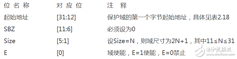
The meaning of the code is shown in the following table.
Regarding bits[31:12] in c6, since the start of the field is an integral multiple of the domain size, the minimum field size is 4 KB, and the bits[11:0] of all domain start addresses are usually 0, and are not set.
MPU programmingProgramming the MPU region can be accomplished by programming the three word registers mapped to memory. The three registers are independent of each other and the program can be accessed separately. The MPU registers are independent of each other, allowing users to easily port existing ARMv6, ARMv7 and CP15 code, making the Cortex-M3 easy to implement backwards compatibility. When porting the existing code for ARMv6 and CP15, you only need to use LDRx and STRx operations instead of MRC and MCR.
An example of updating the MPU region using the CP15 equivalent code is as follows:
R1 = region number
R2 = size/enable
R3 = attributes
R4 = address
MOV R0, #NVIC_BASE
ADD R0, #MPU_REG_CTRL
STR R1, [R0, #0] ;
STR R4, [R0, #4] ;
STRH R2, [R0, #8] ;
STRH R3, [R0, #10] ;
It is worth noting that if the interrupt can be preempted during this period, it will be affected by the MPU area, ie it must be disabled, written and then enabled. This is usually not very useful for context converters, but it is necessary if you need to update elsewhere.
The MPU can contain critical data because it takes more than one bus processing, usually two words, to update, and the result is not "thread safe", ie the interrupt can separate the two words so that the region contains discontinuities Information. At this point, pay attention to the following two issues.
(1) Updating the MPU usually generates an interrupt. This is not only a "read-modify-write" problem, it also affects the situation of "guarantee that the interrupt program does not modify the same area". This is because programming depends on the area code being written to the register, so it knows which area to update. Therefore, in this case, the interrupt must be disabled around each update program.
(2) Updating the MPU using a domain operation will generate an interrupt that will affect the area being updated because only the base address or "size field" is updated. If the new size field has changed, but the base address has not changed, the base address +new_size may overlap in an area that is normally processed by another area.
But for standard OS context conversion code, the user area will be changed, because these areas will be preset to user privilege and user area address, so there is no risk. This means that even if it is interrupted, it will not cause side effects. Therefore, there is no need to disable/enable the code and there is no need to disable the interrupt.
The most common method is to program the MPU from only two locations: the boot code and the context converter. If programming in a unique two locations and the context converter only updates the user area, then the context converter is not a disable because the context converter is already a critical area and the boot code runs when the disable is interrupted.
The KSPOWER`s L series led driver is one ultra slim, constant voltage mode, class 2 class P, 0-10v, triac/phase-cut dimmable rated and designed to operate with any standard brand dimmer switch, like Lutron dimmer etc. The single channel 12Volt 24Volt 36Volt 48Volt led driver is encased in a low profile aluminum enclosure and thin to 24.5mm makes it the perfect choice for under cabinet lights, tape lights and various LED fixtures installations. The UL listed slim LED driver is rated IP67 for indoor or outdoor installations and includes a separate input and output wiring compartment each with knock outs that to enable easy installation. High power factor and efficiency of 88% allows the led driver to operate at low temperatures. The L series LED transformer is Flicker-Free dimmable down to 1% with 0-10V / MLV / ELV / Triac dimmers and is also available in a non-dimmable version. The L series pfc power supply also accept universal 100-277VAC Input Voltage for Residential, Commercial, and Industrial Use.
led street light driver, led driver outdoor, led driver 0 10v dimming, slim led driver, pfc power supply
Shenzhenshi Zhenhuan Electronic Co., Ltd , https://www.szzhpower.com