1 Introduction
The racing brake system is a relatively independent subsystem on the racing system. It is used to withstand the static weight of the car, dynamic impact loads and kinetic energy when absorbing the brakes of the car to achieve braking and control of the car. Its performance directly affects the car's rapid response, safe braking and survivability, which in turn affects the overall performance of the car. This paper designs the hardware and software of the all-electric anti-skid brake controller of the racing car, and finally studies the control law suitable for the racing brake.
2 system hardware circuit design
The racing brake controller consists of an anti-skid controller and a motor drive controller. Both controllers are based on DSP chips. The anti-skid controller is mainly controlled by the slip rate, and outputs a given brake pressure. The DSP chip is used as the CPU, plus the racing wheel and the wheel speed signal conditioning circuit. The motor drive controller mainly adjusts the brake pressure and controls the motor current. It also uses the DSP chip as the CPU, plus the peripheral circuit motor current feedback conditioning circuit, overcurrent protection circuit, brake pressure conditioning circuit, and four sets of three-phase full bridge. The inverter circuit and the like constitute a motor drive controller.
2.1 DSP's minimum system
The DSP's minimum system mainly involves memory expansion, JTAG interface configuration, reset circuit, ADC module settings, and clock circuit design.
1. Off-chip memory expansion. The off-chip memory is to compensate for the lack of internal DSP RAM, and it is also convenient to download the program to the off-chip high-speed StaTIc RAM during the debugging process. The external static random access memory uses CY7C1041CV33. The DSP can use either on-chip program memory or off-chip program memory, as determined by the pin XMP knife MC. JTAG interface. When the program needs to be debugged, the program download is completed through the JTAG interface, which is connected to the parallel port of the PC through the emulator.
2. Reset circuit and clock source module. A low-level reset circuit that generates a power-on reset and a manual reset with a RC circuit generates a reset signal. In addition to a hardware watchdog, its output generates a reset signal WDRST. The two inputs of the power chip are both +5V, and the output is +1.9V and +3.3V power supply for the DSP. The output power supply has two reset signals respectively. When the power supply is unstable or too low, a reset signal will be generated.
3. Hardware configuration of the analog-to-digital conversion ADC module. The analog-to-digital conversion ADC output voltage is 2V, requiring the output to be terminated with a low ESR capacitor of 10μF to the analog ground. If the software is set to external reference mode, ADCREFP can be connected to an external input with a 2V reference voltage and a low ESR capacity of 1μF to 10μF. Otherwise, the accuracy of the AD's internal reference source will be affected.
2.2 Racing front wheel and brake wheel speed signal processing circuit
The anti-skid controller is mainly controlled by the slip ratio to prevent the car from slipping. The pressure reference value is adjusted by the deviation of the slip ratio to track the given slip rate. The anti-skid controller must have a conditioning circuit for the front wheel and brake wheel speed signals, mainly to obtain the feedback slip rate. The racing speed signal is replaced by a free-rolling front wheel speed signal. The speed sensor is installed on the front wheel and the brake wheel of the car. When the wheel rotates, the speed sensor generates an AC signal in the form of a sine wave. Each time the wheel rotates, the speed sensor emits a 50-cycle sinusoidal AC signal. The amplitude of the sinusoidal AC signal varies with the speed of the wheel. The signal is a sine wave signal with a bias voltage of 2.5V, a peak value of 0.3V, and a maximum signal amplitude of no more than 5V. The sine wave signal is converted into a square wave of the same frequency and sent to the capture unit of the DSP, and the count value interval ncapture of the adjacent rising edge of the square wave is captured, and the rotational speed value V of the wheel can be calculated. Since the CPUCLK is 150MHz, the capture time base is one of the timers, n is the division factor of the CPUCLK, and the radius of the wheel is the calculation formula of the wheel speed:
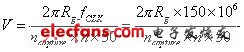 (1)
(1)
The conditioning circuit is shown in Figure 1:
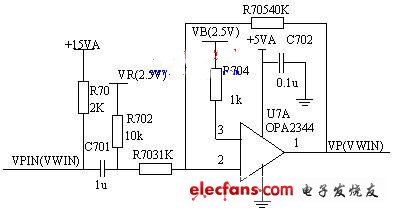
Figure 1 speed conditioning circuit
2.3 logic signal circuit
The motor driver uses ALTERA's MAX7000A series devices to logically process the rotor position of the motor, and selects up to 76 programmable I/0 ports and 100-pin EPM7128AE, which can meet system design requirements. The device EPM7128AE realizes the functions of the three-phase full-bridge inverter circuit trigger signal, over-current protection, forward and reverse, and three-phase full-bridge turn-on and turn-off. There is a logic signal for two motors on a CPLD device EPM7128AE. Since the output of the Hall position sensor CS3020 of the brushless DC motor is an open collector structure, the 2KΩ resistor is pulled up, and the Hall signals SA, SB, SC are sent to the input port of the CPLD. The four terminals of TMS, TCK, TDI and TDO of JTAG interface must be connected with pull-up resistors and then connected to +5V power supply.
2.4 Power drive circuit of brushless DC motor
The power drive circuit of the brushless DC motor uses a three-phase full-bridge inverter circuit composed of six N-channel MOSFETs centered on IR's dedicated driver chip IR2130. The input is a power-ground PWM wave that is sent to the input port of the IR2130, and the output controls the N-channel power-driven transistor MOSFET, thereby driving the brushless DC motor. The use of this driving method is mainly the clever use of the power drive chip IR2130 to form a suspended high-voltage side power supply for the "bootstrap" technology, which simplifies the design of the entire drive circuit and improves the reliability of the system. Moreover, the IR2130 driver chip has a built-in deadband circuit, as well as overcurrent protection and undervoltage protection, which greatly reduces the complexity of the circuit design and further improves the reliability of the system.
Solar energy system, off gird pv system, grid pv system, solar power system, Solar Panel system, on grid solar system, grid tied solar system,20kw solar system
Solar energy system include Solar photovoltaic system: 1. Off grid photovoltaic system mainly consists of solar modules, controllers, and batteries. To supply power to AC loads, it is also necessary to configure an AC inverter. 2. Grid connected photovoltaic power generation system. 3. Distributed photovoltaic power generation system. Distributed power generation or distributed energy supply.
solar cell type
mono crystalline, half cut cell
solar energy pv system include
on grid system, off grid system, hybrid system
solar configuration
solar panel, inverter, battery, bracket cabels, mc4 connector
Product details and pic


Solar Engergy System,Gird Solar Power System,Pv System For Carport,Energy System Off Grid Solar System
PLIER(Suzhou) Photovoltaic Technology Co., Ltd. , https://www.pliersolarpanel.com