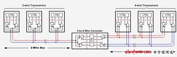
Figure 1 2-4 line converter ensures versatility between half-duplex and full-duplex systems
In order to make the converter run independent of the data rate, we control the turn-on and turn-off of the converter driver and receiver through the logic state of the bus. The bus driver is at every bit interval, allowing the converter to operate independently of the signal data rate.
Simple control logic ensures that drivers D1 and D2 are only enabled by logic low activation of the opposite receiver (ie R1 or R2) output. Because there is a bus fault protection voltage of VFS > 200 mV at the receiver input, both receiver outputs are logic high during bus idle. The inverter gate reverses the logic high to a low state and enables the receiver while the driver is turned off.
In the half-to-full duplex direction ( Figure 2 : left to right), the negative bus voltage at the R1 input activates driver D2 and uses a low state for the driver input. D2 responds by driving the transmission bus with a negative output voltage. When the bus voltage at the R1 input becomes positive, D2 immediately expires. However, its output is high because the fail-safe bias resistor RFS forms the bus voltage VFS.
(Note that during the entire run, the output of R2 is always high, ensuring that R1 remains active and D1 remains inactive.)
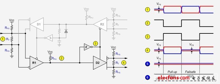
Figure 2 Half-duplex to full-duplex converter timing
In the full-to-half duplex direction (Figure 3: from right to left), the negative bus voltage at the R2 input activates driver D1 and applies a low state to the driver input. D1 responds by driving the two-wire bus with a negative output voltage. When the bus voltage at the R2 input becomes positive, D1 expires after a delay time. During this delay time, D1 uses a negative voltage to drive the bus before high impedance occurs to prevent switching transients at the R1 output.
We recommend that the minimum delay time generated by the RD?CD time constant should be 1.3 times the maximum propagation delay of the driver to compensate for component values, inverter thresholds, and supply voltage tolerances. The required RD value can be determined by Equation 1 for a given capacitance condition:
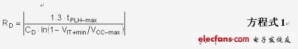
Where tPLH-max is the maximum low-to-high propagation delay of driver D2, VIT+min is the minimum positive input threshold of the Schmitt-triggered inverter, and VCC-max is the maximum supply voltage.
After D1 fails, the bus voltage VFS formed by the fault protection bias resistor RFS has its output still high. When the bus voltage at the R2 input returns to negative, the CD is immediately activated due to the rapid discharge of the CD through the discharge diode DD. The timing diagram shown in Figure 3 shows a remote receiver on the half-duplex bus (here denoted by R ) that converts the negative bus voltage to a low bit. A high bit consists of a low main drive positive bus voltage and a residual fault protection voltage VFS.
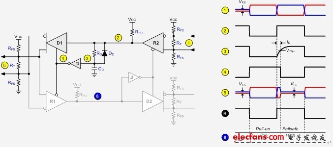
Figure 3 converter timing from full duplex to half duplex
The last converter design shown in Figure 4 uses two full-duplex transceivers: one configured as a half-duplex transceiver and the other in full-duplex mode. The converter has a data rate of up to 200 kbps and is powered by a single 3.3 V supply. Table 1 shows the bill of materials (BOM) for this circuit.
- Specialist at Precision Injection Mold, multi cavity die, plastic injection moulding manufacturing and exporting.
- Providing 3D design service, OEM plastic tool making and ODM injection molding service.
- Manufacturing Multiple Electronics Products, e.g. small solar power bank, Bluetooth speaker, computer equipment.
- Supply Hardware Plastic Parts, e.g. furniture hardware, medical apparatus parts with plastic or steel - plastic or zinc - plastic combined materials.
- Qualified material, qualified processing and precision machines resulting high quality and long life injection mold.
- Producing most kind of plastic material injection parts, PC, PE, HDPE, PP, PS, ABC, Nylon, Rubber etc.
- Supply high quality prototype (3D Printing, CNC processing plus surface treatment and assembly) as for the support of OEM / ODM services.
Plastic Product And Injection Mold
Plastic Product And Injection Mold,Precision Injection Mold, Plastic Injection Products, OEM ODM Injection Molding, Multiple Electronics Products, Hardware Plastic Parts
ZhongShan JITONGLONG Plastic Hardware Co. Ltd. , https://www.toukoo-electronics.com