Broadband CDMA wireless access system and base station design
Broadband fixed wireless access means that some or all of the wireless nodes are used from the switching node to the fixed user terminal. Only the access to the core data network is discussed here. Compared with wired access, fixed wireless access has the following remarkable features: strong adaptability to natural conditions. As long as the user is within the coverage area, no special positioning and precise planning are required. The FWA system is particularly suitable in environments where the terrain and features are not suitable for cable laying and the construction speed is fast. The installation and debugging of user equipment is convenient and flexible, which greatly shortens the construction period. Technically, you can even apply on the same day and open the data service on the same day.
This paper presents a fixed broadband CDMA wireless access system that works in the 2.4G ISM band, and describes the base station system solution. It has the advantages of anti-interference, small size, low cost, and good performance. It is suitable for oilfield, hydraulic, electric power and other industries Data communication private network and data service access in rural areas, suburban areas and other areas.
System composition and working principle
1 System composition
The system consists of five parts: base station, user terminal, transponder, network management system and management computer. Install the base station of the FWA system in the computer room of the local local data exchange center (or near it) in the county town, larger township, or industry private network. Fixed terminals are placed in household distribution areas (such as smaller townships and administrative village centers) or indoors of users, and communicate with base stations in a wireless manner. The user's data communication equipment is directly connected to the 10Base-T interface of the fixed terminal. The base station is connected to the network management PC of the operation and maintenance center through the RS232 interface. The basic configuration of the fixed broadband CDMA wireless access system is shown in Figure 1.

Figure 1 System composition
2 Working principle
The system is a point-to-multipoint microwave communication system that provides users with a low-latency data transmission channel. The system uses TDD duplex mode, CDMA multiple access mode, BPSK modulation, working in the 2.4 ~ 2.4835GHz frequency band. The width of each carrier is 40MHz, and there can be two carriers in total. The base station adopts a three-sector structure, and each sector provides 4 code channels. The three sectors share the same carrier, and each carrier can provide 12 code channels, and each code channel uses different spreading codes. Spreading code uses m sequence or GOLD code. The channel can be fixedly allocated.
The base station is the central node of the wireless link and is connected to the data switch or router through the 10 / 100Base-T interface. The user terminal is a remote node of the wireless link, and is connected to the user equipment through a 10Base-T interface. The wireless channel rate of the user terminal can be set to B, 2B, 2B + D, 6B, 6B + D, and 8B. The transponder is used to extend the communication distance or to bypass obstacles. It is equivalent to two back-to-back user terminals, which work in the master-slave mode, and the various characteristics are the same as the user terminal. The network management system is connected to the base station through the RS-422 interface. The network management software runs in the Windows environment and provides functions such as system parameter setting, system testing, working status monitoring, and fault alarm in the form of graphical interface. The management computer is a notebook computer, runs a terminal management software, and is connected to the user terminal through the RS-232 interface. The terminal management software also runs in the Windows environment, and provides user interface or transponder working parameter setting, working status monitoring, fault diagnosis and other functions in a graphical interface. The management computer is only used when the user terminal or transponder is opened or repaired.
Base station design
1 Overall design
The base station is mainly composed of Ethernet switching and interface conversion module, main control module, CDMA baseband processing module, RF module, network management system and power supply. The overall block diagram is shown in Figure 2.
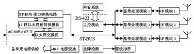
Figure 2 Functional block diagram of the base station
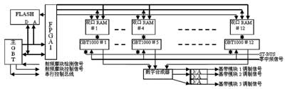
Figure 3 Block diagram of the baseband circuit
A base station consists of 3 sectors. Each sector uses an independent transceiver (radio frequency module), which can be configured with 3 baseband modules, and each baseband module supports 4 channels. The first baseband module card is responsible for the control and supervision of the radio frequency module. The main control module controls 3 baseband modules, and the baseband module completes CDMA baseband processing tasks.
CDMA uses a dedicated CDMA multiple access scheme as shown in Table 1. The spreading code pattern uses m-sequence or GOLD code with a maximum period of 232-1 (m) or 216-1 (GOLD).
The system uses the ST-BUS bus defined by Mitel as the base station baseband circuit data bus. This bus is mainly defined for the 2.048Mbps code rate signal. It specifies a frame structure similar to E1, frame synchronization clock and its naming method, clock and input and output The timing relationship of data, etc. The user data of the baseband module and the main control module are connected to the ST-BUS and connected to the ST-BUS interface conversion circuit, where the ST-BUS signal and the Ethernet bridge input signal are converted. The ST-BUS interface conversion circuit is realized by FPGA, and completes the sequence conversion function.
The RF module works in TDD mode. In the receiving state, the base station signal received by the antenna is sent to a low-noise amplifier for amplification after a band-pass filter and a transceiver switch. The system adopts the method of one frequency conversion, and the radio frequency signal directly becomes zero intermediate frequency after one frequency conversion. The two zero-IF signals of I and Q are sent to the baseband module after low-pass filtering and buffer amplification. In the transmitting state, the baseband spreading signal sent by the baseband processing module is synthesized into one channel by the linear adder, and then shaped and filtered through a low-pass filter, and then sent to the modulator to modulate the carrier wave. The system adopts the method of directly modulating the carrier wave. The baseband module outputs a power control signal (APC) according to the network management command, and controls the gain of the excitation stage and the final stage to control the transmission power.
2 Baseband circuit design
As shown in Figure 3, the baseband circuit is composed of 3 baseband modules, each baseband module supports 4 channels, each channel uses a slice of GBT1000, and the main GBT1000 centrally controls 12 channels. The master GBT controls the slave GBT through the dual-port RAM, including downloading the slave GBT program, sending control commands, reading working parameters and status, etc. The master GBT can operate on one slave GBT individually, or can perform the same operation on multiple slave GBTs at the same time. The master GBT and slave GBT programs are stored in a piece of Flash RAM, which can be hard-coded or modified by the master controller downloading new programs through the serial control bus. The baseband spread spectrum signals output from GBT of the three baseband modules are synthesized by a digital synthesizer and then converted by three D / A chips, and then sent to three radio frequency modules. In a digital synthesizer, each input signal is first multiplied by the corresponding power factor according to its channel rate, and then linearly added. The main GBT is responsible for providing various control signals to the radio frequency module, and detecting the DC indication signal sent back by the radio frequency module through the A / D. The main GBT accepts the instructions of the network management computer through the serial control bus and reports various working parameters and status to the network management computer. The digital synthesizer is completed by FPGA3, the ST-BUS interface conversion circuit is completed by FPGA2, FPGA1, 2, and 3 are all selected by field programmable chip ALTERA EPM7512AE-144, and the dual-port RAM is selected by IDT70V06 chip. D / A selects AD9708 now.
3 RF module design
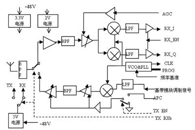
Figure 4 Functional block diagram of the RF module
The functional block diagram of the radio frequency module is shown in Figure 4, which works in TDD mode. In the receiving state, the base station signal received by the antenna is sent to a low-noise amplifier for amplification after a band-pass filter and a transceiver switch. After another filtering, it is further amplified by the second-stage radio frequency amplifier (AGC amplifier). The AGC signal is provided by the baseband card. The mixer performs quadrature down-conversion on the radio frequency signal and outputs I and Q signals. After one down conversion, the radio frequency signal directly becomes zero intermediate frequency. The two zero-IF signals of I and Q are sent to the baseband module after low-pass filtering and buffer amplification. GBT1000 outputs FLL signal, controls the frequency of the reference frequency source, and locks the local oscillator signal generated by the frequency synthesizer to the receiving carrier frequency. In the transmission state, the baseband spread spectrum signal sent by the baseband module is shaped and filtered through a low-pass filter and sent to the modulator to modulate the carrier wave (ie, local oscillator).
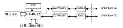
Figure 5 Schematic diagram of Ethernet switch module
The system adopts the method of directly modulating the carrier wave. The modulated signal is pre-amplified by the excitation stage, the out-of-band radiation is suppressed by the band-pass filter, and the power amplifier is amplified by the final stage power amplifier, and then sent to the antenna via the transceiver switch and band-pass filter. The baseband circuit outputs a power control signal (APC) according to the network management command, and controls the gain of the excitation stage and the final stage to control the transmission power. The TX_EN signal controls APC to work only when the data frame is sent, and does not transmit power at other times. The TX_RXb signal is a transceiver control signal. On the one hand, it controls the radio frequency switch to switch between the receiving channel and the transmitting channel. On the other hand, it controls the power supply to only supply power to the working channel to achieve the purpose of power saving. The main technical indicators of the RF circuit are as follows:
â— Input modulation signal multi-level bipolar digital signal, the maximum amplitude is 3V, the rate is 32.768Mcps;
â— After shaping filtering, 99% of the signal energy is concentrated in about 40MHz bandwidth;
◠The carrier frequency is in the 2.4-2.4835GHz frequency band, and the accuracy is not less than 1 × 10⁻⁶;
â— The bandwidth of the modulated signal is about 40MHz;
â— The power control range is 70dB;
â— The output power of the 1dB compression point of the final power is 500mW, and the maximum output power is 200mW;
â— The power detection signal is proportional to the output signal amplitude. When the output power is 500mW, the output level is 5000mV. When the output power is 0mW, the output level is 0mV;
â— The standing wave of the antenna port is not higher than 1.3;
â— The minimum received signal level at the antenna port is -110dBm and the maximum is -40dBm;
â— From the antenna port, the noise figure of the receiver is not higher than 3.0dB;
â— AGC range is not less than 70dB;
â— The output amplitude of the zero-IF signal is 200mV;
â— Transceiver conversion time and power-on time are not more than 10nS
◠The power supply voltage is -48V ± 20% DC.
4 Ethernet switch design
The switch adopts the switch structure with Galileo Technology's ASIC network switch chip GT-48212 as the core. The chip can work in two configuration modes: unmanaged mode and managed mode, and can be expanded into a distributed two-chip frame structure. Figure 5 shows the schematic diagram of the Layer 2 Ethernet switch module, which contains 12 10Mbps ports and 2 10 / 100Mbps adaptive ports. Switches include: switching chips (switching engines), SDRAM, physical layer chips, transformers, crystal oscillators, control logic and peripheral circuits. SDRAM selects MT41LC256K3204 chip, and GT-48212 works in unmanaged mode.
The 12-channel Ethernet bridge in Figure 2 is implemented by 12 dedicated chip bridges RJ017.
5 GBT1000 software design
GBT1000 contains a built-in CPU V6502. The software flow design of master and slave GBT1000 is shown in Figure 6.
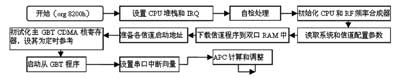
Figure 6-a Main program block diagram of the main GBT1000
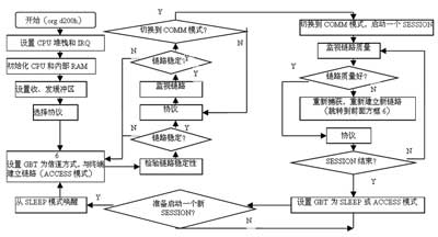
Figure 6-b from GBT1000 program block diagram
Conclusion
This article gives a fixed broadband CDMA wireless access system solution and the design and implementation of the base station, briefly describes the system architecture and working principle. It focuses on the overall design of the base station and the design of each module. After the image transmission test, the system has a good network rate, can transmit audio, images and data in real time, and has good practical application value. And it has the advantages of anti-interference, small size, low cost, good performance, etc., and provides a practical solution for data communication private networks in oil fields, hydraulics, power, and other industries, and in rural and urban suburbs that are not suitable for wired data communication. Program.
Coupletech Co., Ltd supplies a variety of high quality optical components: optical material, lenses, windows, mirror, prisms, filter, IPL - filter. Optical material is including BK7, Fused silica, quartz, CaF2, MgF2, BaF2, Sapphire, ZnSe, a-BBO, LiNbO3, Calcite, and so on. Lens is including Plano Convex Spherical Lens, Double Convex Spherical Lens, Plano Concave Spherical Lens, Double Concave Spherical Lens, Meniscus Spherical Lens, Ball Lens, Rod Lens, Plano Convex Cylindrical Lens and Plano Concave Cylindrical Lens, Achromatic lens and so on. Windows are optical glass with polished faces that are relatively parallel. They are used to protect laser output. Always windows are AR coated, HR coated or PR coated. Mirrors is including Dielectric laser line mirror, Metal coated mirror, Right angle prism mirror, Output coupler, harmonic separator. Prisms are including Right angle prism, Dove prism, Porro prism, Brewster prism, Roof prism and wedge prism. Filter is inclusing Color glass filter, Interference Bandpass filter, Neutral Density Filter-Absorptive and Neutral Density Filter-Reflective.
Coupletech supplies many kinds of Optical Elements with different materials.


Optical Elements,Optical Lenses,Optical Filters,Optical Windows,Optical Mirrors,Optical prisms,ZnSe windows
Coupletech Co., Ltd. , https://www.coupletech.com