CPLD Design of I2C Device Interface IP Core
According to the characteristics of the I2C serial expansion of the single chip microcomputer, in the environment of the EDA software MaxplusII, the AHDL language is used to establish the IP core. This design is realized by using a state machine, and the process of establishing the IP core is explained in detail while the design is given, and it is downloaded to the chip to pass the hardware test verification.
Keywords: Programmable logic device I2C serial expansion IP core
Due to the structural trend of CPLD digital design, IP (Intellectual Property) cores for different levels of CPLD will appear. Each IP core can be reused, which can greatly improve design capabilities and efficiency. Major foreign companies have launched special IP cores, and my country urgently needs to develop its own IP cores. This text gives the design process and result in detail according to the characteristic of I2C main mode serial expansion communication.
1 Introduction to IP Core
IP core refers to: design some commonly used but more complex functional blocks in digital circuits, such as FIR filters, SDRAM controllers, PCI interfaces, etc., into modules that can modify parameters, so that other users can directly call these modules to Avoid duplication of work. As the scale of CPLD/FPGA becomes larger and larger and the design becomes more and more complicated, the use of IP cores is a development trend. Many companies recommend using ready-made or tested megafunction modules and IP cores to enhance existing HDL design methods. When designing complex systems, these megafunction modules and IP cores will undoubtedly greatly reduce design risks and shorten the development cycle. Using these macro function modules and IP cores will spend more time and energy on improving and enhancing system-level products, without the need to redevelop the discovered macro function modules and IP cores. The construction of my country's IP nuclear database is quite urgent, and it is an important goal for the development of the integrated circuit industry.
2 Introduction to the characteristics of I2C serial communication
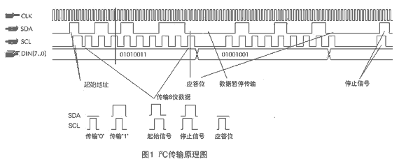
The I2C software and hardware protocol introduced by Philips is very clever. In the single-master I2C bus system, there is only one single-chip microcomputer on the bus, and the rest are peripheral devices with I2C bus. Because there is only one single-chip microcomputer on the bus as the master node, the monolithic system will always occupy the bus, and there will be no competition, and the master node does not need to have its own node address. As long as each peripheral device has its own device address, the two I/O port lines SCL (clock line) and SDA (data line) can virtual I2C bus interface. Data transfer on the I2C bus is shown in Figure 1. Each frame of data transmitted on the bus is 1 byte. After starting the bus, it is required that the other party responds with an acknowledge bit after every 1 byte is transmitted. When sending, the highest bit is sent first. There is a start signal at the beginning of each transfer, and a stop signal at the end. After the bus transfers 1 byte, the transfer can be paused by controlling the clock line. At this time, the SCL can be changed to low level after the response signal to control the bus to pause. The same method can also be used when the master node requires the bus to be suspended. Figure 1 is a situation where the CPLD sends two data, 01010011 and 01001001, to the peripheral I2C device.
3 Establishment of I2C serial extended IP core in MaxplusII environment
MaxplusII is the EDA software used by Altera Corporation in the United States for CPLD. There are many commonly used macro units inside, such as counters, four arithmetic operations, various logic gates, and even ROM, RAM, etc. The specific parameters in these macro units can be set by the user, which is the IP core form mentioned above. It avoids duplication of labor and improves efficiency. What will be designed below is the IP core of the lower computer.
MaxplusII's AHDL (Altera Hard ware DescripTIon Language) is a modular high-level language fully integrated in MaxplusII developed by Altera, which is especially suitable for describing complex combinational logic, group operations, state machines and truth tables. This article uses AHDL to directly generate IP cores.
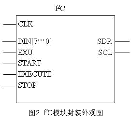
The ultimate goal of the design is to generate the Symbol as shown in Figure 2. The purpose of controlling SDA and SCL is achieved by inputting data, and the signal is transmitted to the I2C device according to the required timing.
The design idea is to use a state machine to implement timing. It mainly includes state machines such as input data latch, start, data transmission, and stop. Through the state machine, in each state, it is determined whether the next state SDA and SCL are high or low. In this way, every timing required by I2C is realized. Since AHDL is used, this state machine is very convenient to implement, and the program is concise and clear. Due to space limitations, only the state machine for data transmission is introduced. The state diagram is shown in Figure 3.
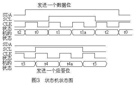
In the following program, Cmd_reg2 is the sending permission temporary storage bit; Sh_reg[] is the data latch, by shifting to the left, the highest data Sh_reg7 is the current data to be sent and stored in SDA_tmp. Through the control program in Figure 3, you can see the detailed process of sending a data bit using the state machine. The program list is as follows:
IF Cmd_reg2 THEN - If "send is allowed", use Sh_reg7 as the current sending bit SDA_tmp = Sh_reg7; ELSE SDA_tmp = VCC; END IF; St.clk = SysClk; St.ena = BaudGen; CASE St IS - control transmission 8 State machine for bit data WHEN t0 => IF Cmd_reg2 OR Cmd_reg3 THEN SDA = SDA_tmp; --Start data transmission SCL = GND; St = t1; ELSE St = t0; END IF; WHEN t1 => SCL = VCC; SDA = SDA_tmp ; St = t1a; WHEN t1a => SCL = VCC; SDA = SDA_tmp; St = t2; WHEN t2 => Sh_reg[7..1] = Sh_reg[6..0]; --Shift the data to the left, take the high-order Sh_reg [0] = GND; Sh_reg[].ena = EXU; SCL = GND; SDA = SDA_tmp; IF Bit[] == 7 THEN - If the 8 bits are transmitted, the response bit will be sent; otherwise, continue to St = t3; ELSE St = t0; END IF; WHEN t3 => --Send response bit SDA =GND; St = t4; WHEN t4 => SDA = GND; SCL = VCC; St = t4a; WHEN t4a => SDA = GND; SCL = VCC; St = t5; WHEN t5 => SCL = GND; St = t6; WHEN t6 => SDA = GND; FINISHED = VCC; St = t0; END CASE; Bit[] = Bit[] + 1; ――- -After one bit is transmitted, the number of transmitted bits plus one
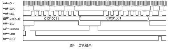
Figure 4 shows the simulation results. After the start signal is given, two 8-bit data are transmitted: each data is followed by a response bit, after the first data request is completed, pause for a period of time, and then transmit the second data; the two data are transmitted. Later, the host sends a stop transmission request, that is, a stop signal is given. These signals fully comply with I2C timing requirements on SDA and SCL. To make the bus transfer rate reach the improved specification, that is, 400 kb/s, because according to the above description, it takes 4 clock cycles to send 1 bit of data, so the given clock is 1600 kHz. In Figure 4, Execute is the execution signal, that is, when it is high, the input data DIN[7..0] is valid; EXU is the send enable signal, and only when it is high, can serial data be sent to the peripheral device ; Start is the start control signal, used to generate a start signal; STOP is used to inform the end of the bus data transmission, and a stop signal occurs.
After the simulation, download the generated pof file to the FPGA board EPM7128SLC84-6 by means of ISP (in-system programming) through the programming cable, with pull-up resistors on the I/O ports SDA and SCL, and two external I2C devices SAA1064 (LED display I2C string In and out of the chip) for testing, the result is that the CPLD uses the I2C IP core, which works normally and can be displayed as required.
References 1 Altera. ALTERA DIGITAL LIBRARY 2000 2 He Limin. Advanced Tutorial of Single Chip Microcomputer. Beijing: Beihang University Press, 2000 3 Zhao Shuguang. Principle, Development and Application of Programmable Logic Devices. Xidian University Press, 2000 4 SAA1064 Product SpecificaTIon Philps.
Cixi Congfeng Fluorine Plastic Co.,Ltd , https://www.cfptfeseal.com