In order to facilitate the testing of 1553B devices, a design and implementation method of 1553B bus test system based on ARM9 platform and FPGA is introduced. The system uses the LPC3250 as a microprocessor and implements the interface logic of the ARM and 1553B protocol chips with the EP1C6Q240C8 chip of the CYCLONE I series. Implement the 1553B driver under the Linux operating system 2.6 kernel. 15 53B protocol chip uses BU-64843T8 to achieve system portability.
With the development of avionics systems, multi-channel data transmission data buses play an increasingly important role in avionics systems. Their main features are centralized control, high real-time requirements, and distributed processing. The 1553B bus is widely used in military and aerospace systems due to its high reliability and flexibility. The traditional 1553B test equipment uses a common computer or an industrial computer as a test platform, and communicates with the device under test through the PCI bus, which causes great inconvenience to the carrying of the test device. The test system described in this paper uses ARM9 as the central processing unit and DDC's BU-64843T7 as the 1553B protocol chip to realize the miniaturization and portability of the system. The application FPGA realizes the conversion of ARM timing and 1553B timing, and adopts the Linux operating system. To ensure that the system is stable and reliable.
1 ARM and FPGA data communication interface design
1. 1 System Hardware Introduction
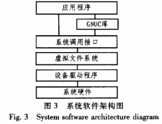
The system hardware consists of LPC3250 core board, external expansion interface circuit, FPGA and 1553B protocol chip. The system architecture is shown in Figure 1.
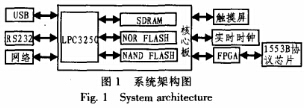
The LPC3250 microprocessor is designed for low-power, high-performance applications. It uses the ARM926EJ-S CPU core to implement 5-stage pipeline processing and Harvard architecture. It can operate at 266 MHz and has powerful data processing capabilities.
The system expands USB, RS232 and network interface for operating system programming and driver, application debugging, and is equipped with real-time clock, which can be powered down. In order to increase its reliability, the system adds ESD chips in multiple places to enhance the antistatic capability of the system.
The FPGA uses Altera's Cyclone I series of EP1C6Q240C8 chips, which have 20 060 logic cells and 288 kb RAM. They support the 3.3V LVTTL/CM OS IO standard and can communicate directly with the ARM without level shifting.
The 1553B protocol chip selects DDC's BU-64843T8 chip. The chip is the world's first chip to integrate the 1553B protocol chip and isolation transformer. Therefore, when the PCB is laid, a large space is saved, so that the system is small and convenient to carry.
1.2 interface circuit design
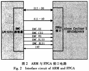
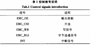
The LPC3250 includes three external memory interfaces, namely a NAND Flash controller, a Secure Digital controller, and an external memory controller (EMC). EMC provides an interface between the system bus and off-chip memory devices for communication with SDRAM, DDR SDRAM, and SRAM devices. The system uses EMC's static RAM interface to communicate with the FPGA. The interface features simple sequence operation and fast interface speed. The FPGA is used to simulate static RAM and perform timing conversion to achieve ARM access to the 1553B chip. Figure 2 is the interface circuit diagram of ARM and FPGA. Since the internal RAM of 1553B chip is 4K*16bit, the data line is 16 bits and the address line is 12 bits. The data bus can be set to 8-bit, 16-bit, and 32-bit by the configuration register of the EMC static memory controller. The system needs to set the lower two bits of the configuration register to 01, the 16-bit bus. Other control signals are described in Table 1.
1. 3 FPGA logic design
If you want to successfully access the 1553B device, you must operate strictly according to the 1553B timing. However, the timing of the EMC is very different from the timing of the 1553B. Therefore, timing conversion is required, which is realized by an FPGA. The control signals of BU-64843T8 mainly include TRANSPARENT/BUFFERED*, STRBD*, SELECT*, RD /WR*, MEM/REG*, IOEN*, READYD*, ADDR_LAT/MEMOE*.RT_AD_LAT*, INT* and other signals.
The TRANSPARENT/BUFFERED* signal is used to set whether the chip works in transparent mode or buffer mode. The 1553B of the system does not need to expand the memory, and it can work in the buffer mode. Therefore, signals such as MEMOE* can be ignored; STRBD* and SELECT * Can be connected together as the chip select signal of the chip; RD/WR* is the read/write signal; MEM/REG* is used to distinguish between accessing internal 4K memory resources or register resources; when IOEN* is valid, the flag chip is processing external access The READYD* signal is very important in this system. When ARM writes, READYD* is valid to indicate that the data is successfully written into the chip. When ARM reads, READYD* is valid to indicate that the data on the data line is valid and can be used; ADDR_LAT is the address lock. The signal is stored, and the signal is set high for the processor that is not multiplexed by the bus; the RT_AD_LAT* signal is the RT address latch signal, and the rising edge of the signal can latch the data at the RT address into the chip, so RT The address does not have to be kept. The INT* signal is used to interrupt the ARM. This signal is connected to the GPIO pin of the ARM via the FPGA. The corresponding GPIO pin is configured as an external interrupt pin.
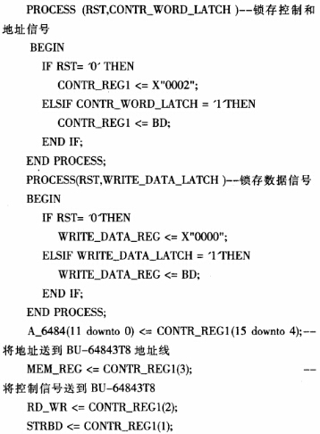
The logic design of the FPCA uses a latching method, that is, all address signals, data signals, read and write, chip select, and EME/REG* signals are directly applied to the bus through the latches, and these signals are always valid during ARM access. Therefore, the ARM needs to perform multiple write operations: first send the data to be written, then send the address and control information to be accessed, and then cyclically read the READYD* signal until it is valid, and then perform the next read and write operation. The relevant VHDL code is as follows:
2 1553B driver development principle and implementation
2.1 file operation interface
Device drivers play a special role in the Linux kernel. They are separate modules that allow a particular hardware to respond to a well-defined internal programming interface, and the user's actions are performed through a standardized set of calls that are independent of the particular driver. Mapping these calls to device-specific operations that act on the actual hardware is the task of the device driver. The system software architecture is shown in Figure 3.
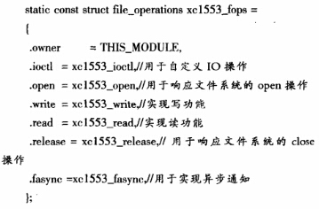
The Linux driver supports three types of devices: character devices, block devices, and network devices. A character device is a device that can be accessed like a byte stream. Character device drivers usually implement open, close, read, and write system calls. The 1553B device of this system belongs to a character device, and its driver mainly includes the following modules: an initialization module, an opening and closing module, a reading and writing module, and an interrupt processing module.
The communication between the driver and the application is mainly through the system function call. Linux provides a unified operation function interface for all device files. Our driver only needs to implement the corresponding function in struct file_operaTIons, including ioctl, read, write, Open, release, fasync function. The specific C language code is as follows:
When the user loads the driver module, a series of initialization work is done in the staTIc int_init xc1553_init(void) function, including device registration, physical address to virtual address mapping, EMC mode configuration, and interrupt handler registration.
When the user unloads the driver module, the driver module and device are unloaded and the interrupt number is released in the staTIc void_exitxc1553_exit(void) function.
2.2 Implementation of the interrupt processing module
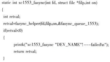
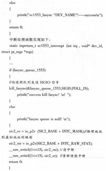
When the 1553B generates an interrupt, it is processed by the interrupt handler registered in the xc1553_init function, and the upper layer application is notified to read and write. The communication between the driver and the application is implemented by means of asynchronous notification. In order to implement asynchronous notification, int fasync_helper(int fd, struct file*filp, int mode, stru ct fasync_struct**fa) and voidkill_fasync(struct fasync_struct**fa, int sig, int band) functions need to be implemented in the driver.
The fasync_helper function is implemented in xc1553_fasync. The function is to create a fasync_struct structure for the current process, and then hang into the fasync queue of the target device. Finally, in the device driver interrupt handler, use the kill_fasync function to send a signal to the queue to notify the upper application. .
The xc1553_fasync function is implemented as follows:
3 Conclusion
The 1553B bus is widely used in the aviation field. The measurement and control equipment based on the 1553B bus is generally bulky and inconvenient to carry. The test system described in this paper can fully realize the functions of the traditional measurement and control equipment, and greatly reduces the size of the equipment and is convenient to carry. After testing, the system has high real-time performance and stable operation, which can meet the requirements of military industry.
RAM/RFM Intermediate Frequency Capacitors
RAM/RFM Intermediate Frequency Capacitors
Intermediate Frequency Capacitors,Induction Heating Capacitors,Furnace Resonant Capacitor
YANGZHOU POSITIONING TECH CO., LTD , https://www.yzpstcc.com