1 Introduction
Modern fisheries mainly use fish finder to detect the distribution of underwater fish resources and increase the output of the fishing industry. The fish finder uses the principle of ultrasonic detection. The ultrasonic probe emits ultrasonic waves of the corresponding frequency according to the requirements. The ultrasonic waves are reflected back after encountering different obstacles in the water and are received by the probe. According to the analysis of the reflection data, the information of the water area is finally obtained. With the development of fish finder, in order to detect more detailed water information, large-angle multi-frequency detection is in order to develop. Therefore, there are generally two ways to increase the angle of ultrasonic detection, mechanical retrace detection of a single probe and multiple probe detection. Since the mechanical retrace circuit of a single probe is complicated in design and the detection interval is limited by the mechanical retrace speed, a multi-probe method is generally adopted. The traditional multi-probe receiving circuit consists of multiple independent single-probe receiving circuits and can only receive ultrasonic waves of one frequency. The hardware is bulky, costly and inefficient. In this paper, a new multi-probe dual-frequency ultrasonic receiving circuit is designed with three dual-frequency probes as an example.
2. Overall circuit overview
This design adopts a new method of time-division switching reception of three dual-frequency ultrasonic probes. The receiving circuit is mainly composed of four parts: preamplifier circuit, switch switching circuit, bandpass filter circuit and post-amplifier circuit. After the signal is initially amplified by the independent preamplifier circuit, the switch switching circuit composed of the analog switch is switched to the required band pass filter circuit for filtering and amplification, and finally amplified by the post-stage amplification circuit to be converted into the AD module of the DSPIC chip. Suitable voltage range.
3. Specific circuit design
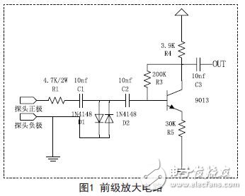
3.1 preamplifier circuit
The function of the preamplifier circuit is isolation and preliminary amplification. Since the ultrasonic probe works in a transceiving manner, the receiving circuit first passes through an isolation circuit. As shown in Figure 1, we use two anti-parallel 1N4148 diodes D1, D2 grounded for isolation purposes. When transmitting, the high voltage pulse signal will discharge directly to the ground through the diode. The diode is equivalent to a short circuit and will not burn out the receiving circuit. When the probe is received, the tiny signal can't make the diode turn on, which is equivalent to the open circuit, and the tiny signal is amplified and received by the subsequent receiving circuit.
The amplifying part adopts a common emitter amplifying circuit built by a 9013 triode, and R3 and R5 are negative feedback resistors, which function to stabilize the bias point of the BJT. The gain of the amplifier circuit is:
Let β=120, and calculate gm is about 0.03. At this time, according to formula 1, the signal gain Av can be calculated to be approximately equal to 61.6.
3.2 Switching Circuit
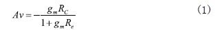
The switch switching circuit consists of a 4066 analog switch that is controlled by the pins of the DSPIC chip. After the transmitting circuit transmits an ultrasonic pulse, the circuit enters a receiving mode.
The chip control analog switch selects which of the three probes will be received, and what the received ultrasonic frequency is, and then begins to receive.
Analog switch switching receives this innovative approach, allowing multiple ultrasonic probes to share a set of post-amplifier circuits. This approach greatly saves circuit cost due to the higher hardware cost of the post-amplifier circuit. The path switching principle is shown in Figure 2:
It is worth noting that it takes a while for the analog switch to be re-stabilized after switching, so it is not suitable for receiving signals during this time. According to the actual measurement, the receiving circuit takes 10 milliseconds to re-stabilize after the switch is switched.
3.3 band pass filter circuit
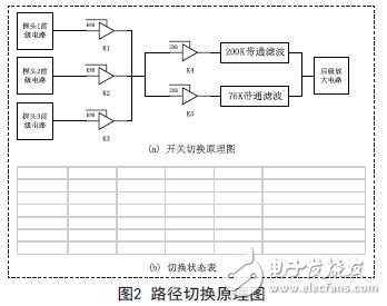
The bandpass filter circuit is composed of two stages of active bandpass filters composed of op amps. The single-stage circuit with a center frequency of 76KHz and its response curve are shown in Figure 3:
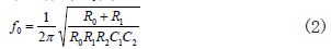
The center frequency 0 f is:
Considering that the values ​​of the resistors and capacitors cannot be arbitrary values, but should be commonly used values, the center frequency of the designed filter has a certain error with the expected center frequency. According to formula 2, when R0=R1 takes 10K, R2 takes 87K, and C1=C2 takes 100p, the maximum voltage gain is 4.35, the center frequency is about 76.3KHz, and the bandwidth is 36.6KHz. When R0=R1 takes 3.3K, When R2 takes 38K and C1=C2 takes 100p, the maximum voltage gain is 5.76, the center frequency is about 201KHz, and the bandwidth is 83.8KHz. Since the absolute errors of the two center frequencies are much smaller than the respective bandwidths, the above circuit parameters are considered to be values. It is reasonable. After the two stages are cascaded, the center frequency is constant, and the voltage gain is the square of a single stage.
3.4 post-amplifier circuit
Due to the large variation of the ultrasonic receiving signal, from a few microvolts to several volts, in order to make full use of the voltage range of the chip AD, a post-amplifier circuit consisting of a logarithmic amplifier and an operational amplifier is innovatively designed, as shown in Fig. 4. Shown. When the input signal is weak, it is equivalent to a linear amplifier with a large gain. When the input signal is strong, it becomes a log amp, and the gain decreases as the input signal increases. The log amp ensures that the ultrasonic receiver circuit has a wide dynamic range. After the AD8310 log amp, the original high frequency signal is converted to the low frequency original signal envelope.
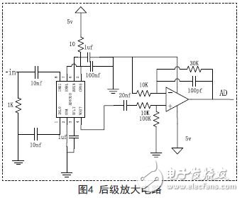
The signal amplitude of the logarithmic amplifier is input to the op amp configured with the non-inverting input for final signal amplitude adjustment. Changing the resistance of the feedback resistor can change the gain of the amplifier circuit. The specific requirement is that the maximum amplitude of the signal finally output to the AD pin should be slightly smaller than the range of the chip AD. Since the ADPIC range of the DSPIC chip is 0-3.3V, here we adjust the feedback resistor so that the final signal has a maximum amplitude of about 3V.
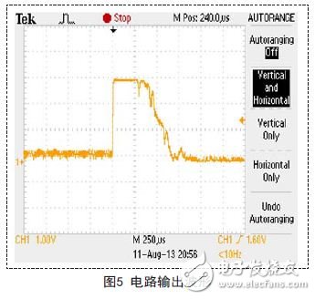
4. Circuit verification
The measured output waveform of the circuit is shown in Figure 5. When the circuit receives a weak reflected signal, the ultrasonic probe generates several microvolts. After amplification and reception by this circuit, the output voltage amplitude is about 3V, slightly less than 3.3V. The AD range meets pre-design requirements.
5. Conclusion
In this scheme, a multi-probe dual-frequency ultrasonic receiving circuit is designed and designed. It can be successfully verified by the experiment that three dual-frequency ultrasonic probes can work normally. The circuit is low in cost, simple and efficient, and has good scalability, providing a new feasible solution for multi-probe and multi-frequency ultrasonic applications.
3520 Phenolic Paper Laminated Tube is formed by hot rolling, baking insulation paper impregnated with phenolic resin under heat and pressure. It is class E (120℃) insulation with high mechanical property. It has good dielectric property in dry conditions.
It is suitable for structural parts of electrical equipments in dry conditions and transformer oil.
Product diameter Φ5mm-Φ5000mm, product length> 20mm or more optional, product wall thickness> 3mm or more optional, product shape cylindrical tube, square tube, hexagonal tube, special-shaped tube, oval tube.
Phenolic Tube,Phenolic Paper Tube,Laminated Paper Tube,Laminated Phenolic Paper Tube
Yingkou Dongyuan Electrical Insulation Board Co.,Ltd , https://www.dy-insulation.com