Abstract: Most electronic devices in modern systems are usually powered by 3.3V or lower, but sometimes it is necessary to provide a voltage of ± 10V to drive an external load (very common in industrial applications). Although some digital-to-analog converters (DACs) can drive loads with a swing of ± 10V, 3.3V DACs are still used in some cases, and the voltage is amplified to ± 10V by an amplifier.
Overview Modern logic systems powered by a 3.3V power supply sometimes run in an industrial environment and may require a voltage drive of ± 10V, such as PLC, transmitter, motor control, etc. One way to meet this need is to choose a DAC that can provide a voltage swing of ± 10V, but a better method is to use a 3.3V DAC and then amplify its output to ± 10V, the reason is: 3.3V DAC is better than ± 10V DAC has higher logic integrity. The 3.3V DAC has a higher-speed logic interface, which can relieve some tasks of the microcontroller to make it handle other tasks. The DAC may be integrated into a large-scale, 3.3V-powered chip (such as a microcontroller) and cannot provide a ± 10V output swing. An external load may require a certain output current to drive, or drive a capacitive load, and a ± 10V DAC cannot meet this requirement. Circuit block diagram The circuit block diagram shown in Figure 1a contains five main parts: DAC, reference source, bias adjustment, reference source buffer and output buffer.
The DAC provides digital-to-voltage conversion with respect to the reference point voltage. The bias circuit adjusts the DAC unipolar transfer function to produce a bipolar output and can calibrate the 0V output point. The reference buffer can provide load isolation and offset adjustment for the reference source. The output buffer superimposes the bias voltage on the signal and provides the required gain to make the output swing meet the required requirements. In addition, the output buffer also provides a certain load drive capability. Circuit Description The circuit shown in Figure 1 and Figure 1a provides a solution to a 3.3V power supply, 16-bit DAC output through amplification to obtain ± 10V output swing. DAC (U2) output range: 0 to 2.5V, connected to the noninverting input of operational amplifier U3. The amplifier provides (1 + 26.25k / 3.75k) or 8 times the in-phase gain. The inverting input of the op amp is connected to + 1.429V, which is generated by the reference and resistor divider network. The gain of the op amp to the inverting input is-(26.25k / 3.75k) or -7. The 0V output of the DAC corresponds to the maximum negative voltage: (0 x 8)-(7 x 1.429) = -10V. The full-scale output of the DAC 2.5V corresponds to the maximum forward voltage: (2.5 x 8)-(7 x 1.429) = + 10V.
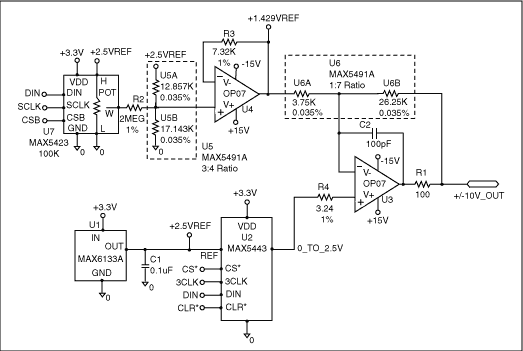
figure 1.
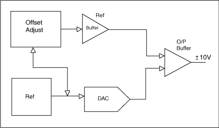
Figure 1a.
The circuit includes the following devices:
U1: MAX6133A, 2.5V reference source U2: MAX5443, 16-bit, 3.3V powered serial DAC U3 and U4: OP07A, precision operational amplifier, ± 15V power supply U5: MAX5491A, precision resistor network with ESD protection, 3: 4 Voltage division ratio U6: MAX5491A, precision resistor network with ESD protection, 1: 7 voltage division ratio U7: MAX5423, 100k, 256-level, non-volatile digital potentiometer reference source 2.5V reference is both the DAC reference voltage In order to generate + 1.429V voltage. These two functions use the same reference source. Therefore, any tracking error between these two voltages will affect the zero offset voltage. Therefore, the common mode error will only affect the full-scale gain of the output, and the gain is generally not a very critical parameter. . The choice of 2.5V as the main reference is because this voltage is very versatile, and it is suitable for 3.3V and 5V power supply. Considering the excellent performance of the device itself, we chose the MAX6133A in a small µMAX® package. The important parameters of the device include: output voltage accuracy (± 0.06%), temperature coefficient (7ppm / ° C) and long-term stability (145ppm / 1kHrs). The most important parameter in digital-to-analog converter industrial control applications is the zero offset error. In this case, the unipolar output of the MAX5443 has ± 2 LSB offset error and ± 10 LSB gain error. These indicators are sufficient to meet the needs of most applications. In order to convert the DAC output to a bipolar signal, a bias circuit is usually used to convert the zero point of the DAC to -10V (negative full-scale), and the intermediate code to 0V. At this time, the mid-code error of the DAC is the sum of zero offset and gain error, not ± 2 LSB. Some applications may not accept this indicator, so we used a digital potentiometer to calibrate its zero output again. Operational amplifier Operational amplifier U4 is placed as a reference buffer between the reference voltage divider resistor network (U5) and the operational amplifier (U3) gain resistor network. If more than one DAC is used in the system, these DACs can share the buffer output. The operational amplifier U3 amplifies the DAC voltage and provides a bias for it. The choice and configuration of the operational amplifier is determined by the load requirements. The following indicators should be considered: Maximum voltage swing Maximum drive current Capacitive load short-circuit protection ESD protection In this example, OP07A can provide a ± 10V / 10mA drive for the load, and the R1 and C2 networks allow the op amp to drive larger capacitive loads.
The operational amplifier parameters that affect system accuracy are VOS (25µV) and IOS (2nA). The impact of IB (2nA) can be offset by R3 and R4. When the equivalent resistance of each input terminal of the operational amplifier is the same, the influence of IB can be eliminated. OP07A's 0.1V / µS slew rate may limit the system slew rate, but there are often no problems in industrial control applications. Resistor network Resistor network U5 (3: 4 ratio) reduces the + 2.5V reference voltage to + 1.429V, and resistor network U6 (1: 7 ratio) sets the gain of operational amplifier U3. The more important parameters are the initial proportional error (0.035%) and the proportional temperature coefficient (5ppm / ° C). The MAX5491 was chosen because the device has ESD protection of ± 2kV, which is very critical, because one end of U6 may be exposed outside the board and need to withstand the impact of ESD discharge. Digital Potentiometer This system uses the MAX5434 256-level digital potentiometer to adjust the zero offset error. The device has a nonvolatile memory that can maintain the offset value after the power is turned off. The resistor network composed of U7, U5 and R2 provides an adjustment range of approximately ± 100 LSB at 0V. Analysis The PSPICE sensitivity analysis of this circuit shows that the maximum zero offset error is 13 LSB, which can be corrected using a digital potentiometer. The temperature analysis results show that the total temperature drift error is 0.126 LSB / ° C. When the temperature changes by 100 ° C, there is an offset error of 12.6 LSB. It is within the allowable range for most applications.
Table 1. Sensitivity analysis, zero output, initial error (in LSB)
Table 2. Sensitivity analysis, zero output, temperature error (in LSB / ° C)
Overview Modern logic systems powered by a 3.3V power supply sometimes run in an industrial environment and may require a voltage drive of ± 10V, such as PLC, transmitter, motor control, etc. One way to meet this need is to choose a DAC that can provide a voltage swing of ± 10V, but a better method is to use a 3.3V DAC and then amplify its output to ± 10V, the reason is: 3.3V DAC is better than ± 10V DAC has higher logic integrity. The 3.3V DAC has a higher-speed logic interface, which can relieve some tasks of the microcontroller to make it handle other tasks. The DAC may be integrated into a large-scale, 3.3V-powered chip (such as a microcontroller) and cannot provide a ± 10V output swing. An external load may require a certain output current to drive, or drive a capacitive load, and a ± 10V DAC cannot meet this requirement. Circuit block diagram The circuit block diagram shown in Figure 1a contains five main parts: DAC, reference source, bias adjustment, reference source buffer and output buffer.
The DAC provides digital-to-voltage conversion with respect to the reference point voltage. The bias circuit adjusts the DAC unipolar transfer function to produce a bipolar output and can calibrate the 0V output point. The reference buffer can provide load isolation and offset adjustment for the reference source. The output buffer superimposes the bias voltage on the signal and provides the required gain to make the output swing meet the required requirements. In addition, the output buffer also provides a certain load drive capability. Circuit Description The circuit shown in Figure 1 and Figure 1a provides a solution to a 3.3V power supply, 16-bit DAC output through amplification to obtain ± 10V output swing. DAC (U2) output range: 0 to 2.5V, connected to the noninverting input of operational amplifier U3. The amplifier provides (1 + 26.25k / 3.75k) or 8 times the in-phase gain. The inverting input of the op amp is connected to + 1.429V, which is generated by the reference and resistor divider network. The gain of the op amp to the inverting input is-(26.25k / 3.75k) or -7. The 0V output of the DAC corresponds to the maximum negative voltage: (0 x 8)-(7 x 1.429) = -10V. The full-scale output of the DAC 2.5V corresponds to the maximum forward voltage: (2.5 x 8)-(7 x 1.429) = + 10V.
figure 1.
Figure 1a.
The circuit includes the following devices:
U1: MAX6133A, 2.5V reference source U2: MAX5443, 16-bit, 3.3V powered serial DAC U3 and U4: OP07A, precision operational amplifier, ± 15V power supply U5: MAX5491A, precision resistor network with ESD protection, 3: 4 Voltage division ratio U6: MAX5491A, precision resistor network with ESD protection, 1: 7 voltage division ratio U7: MAX5423, 100k, 256-level, non-volatile digital potentiometer reference source 2.5V reference is both the DAC reference voltage In order to generate + 1.429V voltage. These two functions use the same reference source. Therefore, any tracking error between these two voltages will affect the zero offset voltage. Therefore, the common mode error will only affect the full-scale gain of the output, and the gain is generally not a very critical parameter. . The choice of 2.5V as the main reference is because this voltage is very versatile, and it is suitable for 3.3V and 5V power supply. Considering the excellent performance of the device itself, we chose the MAX6133A in a small µMAX® package. The important parameters of the device include: output voltage accuracy (± 0.06%), temperature coefficient (7ppm / ° C) and long-term stability (145ppm / 1kHrs). The most important parameter in digital-to-analog converter industrial control applications is the zero offset error. In this case, the unipolar output of the MAX5443 has ± 2 LSB offset error and ± 10 LSB gain error. These indicators are sufficient to meet the needs of most applications. In order to convert the DAC output to a bipolar signal, a bias circuit is usually used to convert the zero point of the DAC to -10V (negative full-scale), and the intermediate code to 0V. At this time, the mid-code error of the DAC is the sum of zero offset and gain error, not ± 2 LSB. Some applications may not accept this indicator, so we used a digital potentiometer to calibrate its zero output again. Operational amplifier Operational amplifier U4 is placed as a reference buffer between the reference voltage divider resistor network (U5) and the operational amplifier (U3) gain resistor network. If more than one DAC is used in the system, these DACs can share the buffer output. The operational amplifier U3 amplifies the DAC voltage and provides a bias for it. The choice and configuration of the operational amplifier is determined by the load requirements. The following indicators should be considered: Maximum voltage swing Maximum drive current Capacitive load short-circuit protection ESD protection In this example, OP07A can provide a ± 10V / 10mA drive for the load, and the R1 and C2 networks allow the op amp to drive larger capacitive loads.
The operational amplifier parameters that affect system accuracy are VOS (25µV) and IOS (2nA). The impact of IB (2nA) can be offset by R3 and R4. When the equivalent resistance of each input terminal of the operational amplifier is the same, the influence of IB can be eliminated. OP07A's 0.1V / µS slew rate may limit the system slew rate, but there are often no problems in industrial control applications. Resistor network Resistor network U5 (3: 4 ratio) reduces the + 2.5V reference voltage to + 1.429V, and resistor network U6 (1: 7 ratio) sets the gain of operational amplifier U3. The more important parameters are the initial proportional error (0.035%) and the proportional temperature coefficient (5ppm / ° C). The MAX5491 was chosen because the device has ESD protection of ± 2kV, which is very critical, because one end of U6 may be exposed outside the board and need to withstand the impact of ESD discharge. Digital Potentiometer This system uses the MAX5434 256-level digital potentiometer to adjust the zero offset error. The device has a nonvolatile memory that can maintain the offset value after the power is turned off. The resistor network composed of U7, U5 and R2 provides an adjustment range of approximately ± 100 LSB at 0V. Analysis The PSPICE sensitivity analysis of this circuit shows that the maximum zero offset error is 13 LSB, which can be corrected using a digital potentiometer. The temperature analysis results show that the total temperature drift error is 0.126 LSB / ° C. When the temperature changes by 100 ° C, there is an offset error of 12.6 LSB. It is within the allowable range for most applications.
Table 1. Sensitivity analysis, zero output, initial error (in LSB)
| Ref Design | Component | DescripTIon | Error Source | Error Value | Error Units | SensiTIvity | SensiTIvity Units | Output Error (LSBs) |
| U1 | MAX6133A | 2.5V Ref | Output Accuracy | 0.06 | % | -2.74E-04 | LSBs /% | 0.00 |
| U2 | MAX5443 | 16 bit DAC | Gain Error | 5 | LSBs | 1.00E + 00 | LSB / LSB | 5.00 |
| U3 | OP07A | OpAMp | VOS | 25 | µV | -2.62E + 04 | LSB / V | 0.66 |
| U3 | OP07A | OpAMp | IOS | 2 | nA | 8.55E + 07 | LSB / A | 0.17 |
| U3 | OP07A | OpAMp | IB | 2 | nA | 1.08E + 06 | LSB / A | 0.00 |
| U4 | OP07A | OpAMp | VOS | 25 | µV | -2.29E + 04 | LSB / V | 0.57 |
| U4 | OP07A | OpAMp | IOS | 2 | nA | 1.68E + 08 | LSB / A | 0.34 |
| U4 | OP07A | OpAMp | IB | 2 | nA | 8.10E + 03 | LSB / A | 0.00 |
| U5 | MAX5491A | Res Network | RaTIo Tolerance | 0.035 | % | 1.40E + 02 | LSB /% | 4.90 |
| U6 | MAX5491A | Res Network | Ratio Tolerance | 0.035 | % | 4.09E + 01 | LSB /% | 1.43 |
| Total | 13.07 | |||||||
Table 2. Sensitivity analysis, zero output, temperature error (in LSB / ° C)
| Ref Design | Component | Description | Error Source | Error Value | Error Units | Sensitivity | Sensitivity Units | Output Error (LSB / ° C) |
| U1 | MAX6133A | 2.5V Ref | Output Temp Co | 7 | ppm / ° C | 2.74E-04 | LSBs /% | 1.92E-07 |
| U2 | MAX5443 | 16 bit DAC | Gain Temp Co | 0.1 | ppm / ° C | 5.00E-02 | LSB /% | 5.00E-07 |
| U3 | OP07A | OpAMp | VOS Temp Co | 0.6 | µV / ° C | -2.62E + 04 | LSB / V | 1.57E-02 |
| U3 | OP07A | OpAMp | IOS Temp Co | 25 | pA / ° C | 8.55E + 07 | LSB / A | 2.14E-03 |
| U3 | OP07A | OpAMp | IB Temp Co | 25 | pA / ° C | 1.08E + 06 | LSB / A | 2.70E-05 |
| U4 | OP07A | OpAMp | VOS Temp Co | 0.6 | µV / ° C | -2.29E + 04 | LSB / V | 1.38E-02 |
| U4 | OP07A | OpAMp | IB Temp Co | 25 | pA / ° C | 1.68E + 08 | LSB / A | 4.20E-03 |
| U4 | OP07A | OpAMp | IB Temp Co | 25 | pA / ° C | 8.10E + 03 | LSB / A | 2.02E-07 |
| U5 | MAX5491A | Res Network | Ratio Temp Co | 5 | ppm / ° C | 1.40E + 02 | LSB /% | 7.00E-02 |
| U6 | MAX5491A | Res Network | Ratio Tamp Co | 5 | ppm / ° C | 4.09E + 01 | LSB /% | 2.05E-02 |
| Total | 1.26E-01 | |||||||
Disposable Cleanroom Swab,Lint Free Cleanroom Swab,Cleanroom Polyester Head Swab ,Polyester Tip Cleanroom Swab
Miraclean Technology Co., Ltd. , https://www.mrccleanroom.com