Abstract: A two-stage 1.9GHz monolithic low-noise amplifier (LNA) with a measured noise figure of 2.3dB and an associated gain of 15dB was fabricated in a standard silicon bipolar transistor array. It dissipates 5.2mW from a 3V supply including the bias circuitry. Input return loss and isolaTIon are -9dB and -20dB, respecTIvely.
© 1998 IEEE. Reprinted, with permission, from 1998 IEEE Microwave and Guided Wave Letters, Vol. 3, No. 3, pp. 136-137 I. IntroducTIonIn portable communicaTIon equipment, such as cellular phones and digital cordless phones, manufacturers are trying to replace as many discrete devices as possible with high-density ICs to be competitive in size, weight, power dissipation, and price. In a number of recent papers low power LNAs for S-band have been described [1,2,3] These LNAs were fabricated using some sophisticated GaAs full-custom processes. Since the high frequency performance of state-of-the-art silicon bipolar processes are continuously improving lowcost semi-custom arrays with a limited choice of components provide a reasonable solution for RF applications.
In order to demonstrate such a solution, we present in this letter a very low-power monolithic 1.9GHz silicon LNA which draws a total current of 1.75mA including bias circuit. II. Circuit Design A schematic of the two-stage LNA is shown in Figure 1. The circuit employs a high-gain common-emitter stage (Q1-RL) and a emitter-follower output stage (Q2-Q3). This approach eliminates the need for coupling capacitors. The current of the first stage is set by a resistive parallel feedback (R3 and R4), which is connected to the external matching inductor (L1) such that no noise degradation occurs. Thus, only a single supply voltage is required. This feedback also improves both the bias and RF stability of the amplifier.
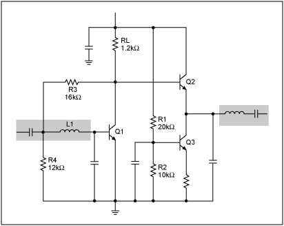
Figure 1. Simplified schematic of the LNA (gray area: off-chip matching).
The circuit was simulated with Spice and with a linear simulator based on measured S- and noise parameter data of the active device. Good agreement between simulated and measured performance is found as shown in Figure 2.
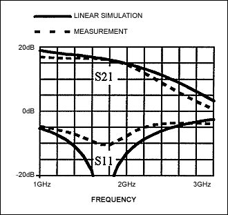
Figure 2. Simulated vs. measured gain and input return loss. III. MeasurementsThe circuit was fabricated on a "Quickchip" transistor array with the Maxim GST-2 foundry process. Figure 3 shows the gain and noise figure of the circuit measured with the HP8970B / HP8971C noise figure meter. The amplifier shows a rather flat frequency response of the noise figure from 700MHz up to 2GHz. The best 50Ω noise figure of 2.3dB is achieved between 1.7 and 2.3 GHz. Note that the active device has a minimum noise figure of 1.5dB at 1.9GHz.
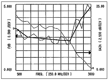
Figure 3. Measured gain and noise figure (VCC = 3V, ICC = 1.75mA (bold line: average noise figure).
The small signal gain is larger than 15dB up to 2GHz at the nominal bias of 3V. The corresponding gain / DC-power figure of merit is 2.9dB / mW. Compared to other L-band LNAs, this design shows low power consumption and a competitive noise figure as seen from Figure 4.
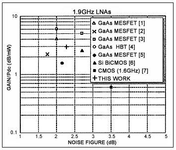
Figure 4. Gain to Dc Power ratio plotted versus noise figure for several state-of-the-art L- and S-band LNAs.
The noise figure is also quite insensitive to bias voltage variations. Varying the supply voltage from 2.7 to 5V the noise figure remains between 2.2 and 2.5dB.
The designed amplifier has a measured -1dB input compression point of -24dBm, which equals an output compression point of -9dBm. The third order intermodulation intercept point is measured at -21dBm input power. This is adequate for DECT handheld terminal.
Figure 5 shows a photograph of the lower right part of the 1.9 x 1.8mm² large chip containing the LNA. In Figure 6 the chip can be seen as mounted on the substrate and bonded to the printed input and output matching inductors.
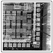
Figure 5. shows a photograph of the lower right part of the 1.9 x 1.8 mm² large chip containing the LNA. In Fig. 6 the chip can be seen as mounted on the substrate and bonded to the printed input and output matching inductors.
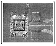
Figure 6. Photograph of the Quickchip mounted on the test substrate. On the right are the printed inductors for input and output matching. IV. ConclusionsA silicon bipolar low power LNA for 1.9GHz has been designed and tested. It shows a noise figure of 2.3 dB along with a 15dB gain. The power consumption is only 5.2mW resulting in a high gain / DC-power figure of merit of 2.9dB / mW. The design was done on a transistor array showing almost no performance degradation relative to full custom design . V. Acknowledgement The authors wish to acknowledge MAXIM for providing access to their GST-2 Quickchip technology.
References Heaney, F. McGrath, P. O'Sullivan, C. Kermarrec, "Ultra low power low noise amplifiers for wireless communications", IEEE 1993 GaAs IC Symposium, pp. 49-51
M. Nakatsugawa, Y. Yamaguchi, M. Muraguchi, "An L-band ultra low power consumption monolithic low noise amplifier", IEEE 1993 GaAs IC Symposium, pp. 1745-1750
U. Lott, "2 GHz monolithic low noise amplifier using lower than 1 V supply voltage", 1997 Wireless Communications Conference, pp. 138-140
KW Kobayashi, AK Owi, LT Tran, DC Streit, "Ultra-low dc power GaAs HBT S- and C-band low noise amplifiers for portable wireless applications", IEEE Trans. MTT, vol. 43, no. 12, pp. 3055-3061, Dec. 1995
KR Cioffi, "Monolithic L-band amplifiers operating at milliwatt and sub-milliwatt dc power consumptions", IEEE 1992 Microwave and Millimeter-Wave Monolithic Circuits Symposium, pp. 9-13
N. Suematsu, M. Ono, S. Kubo, H. Sato, Y. Iyama, O. Ishida, "L-Band internally matched Si-MMIC low noise amplifier", IEEE 1996-S. Int. Microwave Symp. Digest, pp. 1225-1228
DK Shaeffer, TH Lee, "A 1.5 V, 1.5-GHz CMOS low noise amplifier", IEEE Journal of Solid-State Circuits, vol. 32, no. 5, pp. 745-759, May 1997
© 1998 IEEE. Reprinted, with permission, from 1998 IEEE Microwave and Guided Wave Letters, Vol. 3, No. 3, pp. 136-137 I. IntroducTIonIn portable communicaTIon equipment, such as cellular phones and digital cordless phones, manufacturers are trying to replace as many discrete devices as possible with high-density ICs to be competitive in size, weight, power dissipation, and price. In a number of recent papers low power LNAs for S-band have been described [1,2,3] These LNAs were fabricated using some sophisticated GaAs full-custom processes. Since the high frequency performance of state-of-the-art silicon bipolar processes are continuously improving lowcost semi-custom arrays with a limited choice of components provide a reasonable solution for RF applications.
In order to demonstrate such a solution, we present in this letter a very low-power monolithic 1.9GHz silicon LNA which draws a total current of 1.75mA including bias circuit. II. Circuit Design A schematic of the two-stage LNA is shown in Figure 1. The circuit employs a high-gain common-emitter stage (Q1-RL) and a emitter-follower output stage (Q2-Q3). This approach eliminates the need for coupling capacitors. The current of the first stage is set by a resistive parallel feedback (R3 and R4), which is connected to the external matching inductor (L1) such that no noise degradation occurs. Thus, only a single supply voltage is required. This feedback also improves both the bias and RF stability of the amplifier.
Figure 1. Simplified schematic of the LNA (gray area: off-chip matching).
The circuit was simulated with Spice and with a linear simulator based on measured S- and noise parameter data of the active device. Good agreement between simulated and measured performance is found as shown in Figure 2.
Figure 2. Simulated vs. measured gain and input return loss. III. MeasurementsThe circuit was fabricated on a "Quickchip" transistor array with the Maxim GST-2 foundry process. Figure 3 shows the gain and noise figure of the circuit measured with the HP8970B / HP8971C noise figure meter. The amplifier shows a rather flat frequency response of the noise figure from 700MHz up to 2GHz. The best 50Ω noise figure of 2.3dB is achieved between 1.7 and 2.3 GHz. Note that the active device has a minimum noise figure of 1.5dB at 1.9GHz.
Figure 3. Measured gain and noise figure (VCC = 3V, ICC = 1.75mA (bold line: average noise figure).
The small signal gain is larger than 15dB up to 2GHz at the nominal bias of 3V. The corresponding gain / DC-power figure of merit is 2.9dB / mW. Compared to other L-band LNAs, this design shows low power consumption and a competitive noise figure as seen from Figure 4.
Figure 4. Gain to Dc Power ratio plotted versus noise figure for several state-of-the-art L- and S-band LNAs.
The noise figure is also quite insensitive to bias voltage variations. Varying the supply voltage from 2.7 to 5V the noise figure remains between 2.2 and 2.5dB.
The designed amplifier has a measured -1dB input compression point of -24dBm, which equals an output compression point of -9dBm. The third order intermodulation intercept point is measured at -21dBm input power. This is adequate for DECT handheld terminal.
Figure 5 shows a photograph of the lower right part of the 1.9 x 1.8mm² large chip containing the LNA. In Figure 6 the chip can be seen as mounted on the substrate and bonded to the printed input and output matching inductors.
Figure 5. shows a photograph of the lower right part of the 1.9 x 1.8 mm² large chip containing the LNA. In Fig. 6 the chip can be seen as mounted on the substrate and bonded to the printed input and output matching inductors.
Figure 6. Photograph of the Quickchip mounted on the test substrate. On the right are the printed inductors for input and output matching. IV. ConclusionsA silicon bipolar low power LNA for 1.9GHz has been designed and tested. It shows a noise figure of 2.3 dB along with a 15dB gain. The power consumption is only 5.2mW resulting in a high gain / DC-power figure of merit of 2.9dB / mW. The design was done on a transistor array showing almost no performance degradation relative to full custom design . V. Acknowledgement The authors wish to acknowledge MAXIM for providing access to their GST-2 Quickchip technology.
References Heaney, F. McGrath, P. O'Sullivan, C. Kermarrec, "Ultra low power low noise amplifiers for wireless communications", IEEE 1993 GaAs IC Symposium, pp. 49-51
M. Nakatsugawa, Y. Yamaguchi, M. Muraguchi, "An L-band ultra low power consumption monolithic low noise amplifier", IEEE 1993 GaAs IC Symposium, pp. 1745-1750
U. Lott, "2 GHz monolithic low noise amplifier using lower than 1 V supply voltage", 1997 Wireless Communications Conference, pp. 138-140
KW Kobayashi, AK Owi, LT Tran, DC Streit, "Ultra-low dc power GaAs HBT S- and C-band low noise amplifiers for portable wireless applications", IEEE Trans. MTT, vol. 43, no. 12, pp. 3055-3061, Dec. 1995
KR Cioffi, "Monolithic L-band amplifiers operating at milliwatt and sub-milliwatt dc power consumptions", IEEE 1992 Microwave and Millimeter-Wave Monolithic Circuits Symposium, pp. 9-13
N. Suematsu, M. Ono, S. Kubo, H. Sato, Y. Iyama, O. Ishida, "L-Band internally matched Si-MMIC low noise amplifier", IEEE 1996-S. Int. Microwave Symp. Digest, pp. 1225-1228
DK Shaeffer, TH Lee, "A 1.5 V, 1.5-GHz CMOS low noise amplifier", IEEE Journal of Solid-State Circuits, vol. 32, no. 5, pp. 745-759, May 1997
High Power High Voltage Power Supply
Hv Power Supply,High Voltage Power Supply 100Kv,Adjustable High Voltage Power Supply,Adjustable High Voltage Power Supply
Yangzhou IdealTek Electronics Co., Ltd. , https://www.idealtekpower.com