The diode consists of a die, a package and two electrodes. The die is a PN junction. A lead is drawn at each end of the PN junction, and a plastic diode, glass or metal material is used as the package to form a crystal diode, as shown in the following figure. The electrode drawn in the P region is referred to as a positive electrode or an anode, and the electrode extracted in the N region is referred to as a negative electrode or a cathode. 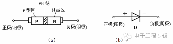
1.1. Volt-ampere characteristics of a diode The volt-ampere characteristic of a diode is the relationship between the voltage applied across the diode and the current flowing through the diode. The curve used to qualitatively describe the relationship between the two is called the volt-ampere characteristic curve. The volt-ampere characteristics of the silicon diode observed by the transistor plotter are shown in the figure below. 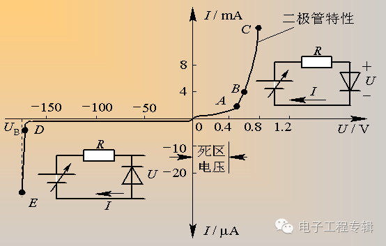
1.2. Forward characteristics 1) When the applied forward voltage is small, the diode exhibits a large resistance, the forward current is almost zero, and the curve OA segment is called a non-conducting region or a dead region. Generally, the dead zone voltage of the silicon tube is about 0.5 volt, and the dead zone voltage of é”— is about 0.2 volt. This voltage value is also called the threshold voltage or the threshold voltage. 2) When the applied forward voltage exceeds the deadband voltage, the electric field in the PN junction is almost cancelled, the resistance of the diode is small, the forward current begins to increase, and enters the forward conduction region, but the voltage is not proportional to the current, for example, AB. segment. The forward current increases rapidly with the increase of the applied voltage. For example, the characteristic curve of the BC section is steep, and the volt-ampere relationship is approximately linear, and is in a fully conducting state. 3) The forward voltage at both ends after the diode is turned on is called the forward voltage drop (or tube voltage drop) and is almost constant. The tube pressure drop of the silicon tube is about 0.7V, and the tube pressure drop of the manifold tube is about 0.3V. 1.3. Inverse characteristics 1) When the diode is subjected to a reverse voltage, the internal electric field of the PN junction is strengthened, and the diode exhibits a large resistance, and at this time, there is only a small reverse current. For example, the OD segment of the curve is called the reverse cut-off region, and the current is called the reverse saturation current. In practical applications, the smaller the reverse current, the larger the reverse resistance of the diode and the better the reverse cutoff performance. Generally, the reverse saturation current of a silicon diode is below several tens of microamps, the germanium diode is several hundred microamperes, and the high power diode is slightly larger. 2) When the reverse voltage increases to a certain value (point D in the figure), the reverse current sharply increases and enters the reverse breakdown region. The voltage corresponding to point D is called the reverse breakdown voltage. If the current is too large after the diode is broken down, the tube will be damaged. Therefore, the reverse voltage of the diode must not exceed the breakdown voltage except for the Zener diode.
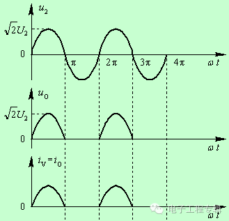
2. Rectifier circuit 2.1, unidirectional half-wave rectifier circuit diode is like an automatic switch. When u2 is positive half cycle, it automatically turns on the power supply and load. When u2 is negative half cycle, it automatically cuts off the power supply and load. Therefore, as shown in the figure below, the pulsating DC voltage uo with the same direction and size change on the load is shown in the figure below. Since this circuit has an output only in the positive half cycle of u2, it is called a half-wave rectification circuit. If the polarity of the rectifier diode is reversed, a negative DC ripple voltage can be obtained.
2.2, full wave rectifier circuit
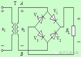
Rectification principle: Set the voltage on the secondary side of the transformer to be: 1) When u2 is positive half cycle, the potential at point A is the highest, the potential at point V is the lowest, the diodes V1 and V3 are turned on, V2 and V4 are turned off, and the current path is A→V1. →RL→V3→B. 2) When u2 is negative half cycle, the potential at point B is the highest, the potential at point A is the lowest, diodes V2 and V4 are on, V1 and V3 are off, and the current path is B→V2→RL→V4→A. It can be seen that in a period of change of u2, the current from top to bottom always flows through the load RL, and the waveform of the voltage and current is a full-wave pulsating DC voltage and current, as shown in the following figure.

3. The filter circuit rectifier circuit converts the alternating current into pulsating direct current, but it contains a large amount of alternating current components (called ripple voltage). To do this, it is necessary to filter out the AC components in the pulsating DC, a process called filtering. 3.1. Characteristics of Capacitor Filter Capacitor Filtering: 1) The average value of the output voltage is related to the size of the filter capacitor C and the load resistor RL. The larger the capacitance of C or the resistance of RL, the slower the discharge speed and the output voltage. The larger the filter, the better the filtering effect. 2) When a large-capacity filter capacitor is used, the instantaneous charging current when the power is turned on is particularly large. The capacitor filter has a simple structure, a high DC voltage of the load, and a small ripple, but the output characteristics are poor, so it is suitable for a case where the load voltage is high and the load does not change much. 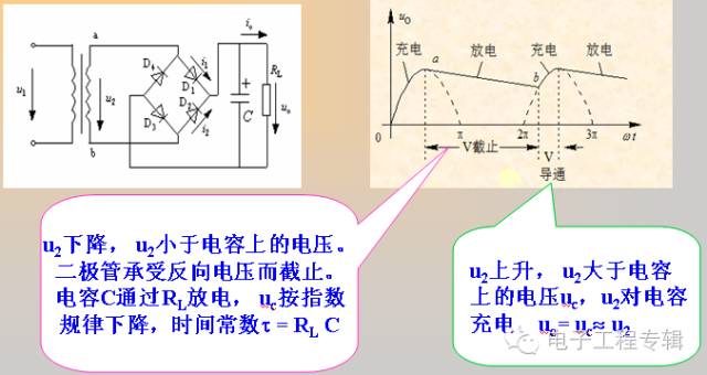
Parameter selection: 1) Output voltage: UL=U2 (half-wave) UL=1.2*U2 (full-wave or bridge) 2) Capacitor selection: C>=(0.03~0.05)/RL3) Diode selection: Urm= 1.41*U23.2, Inductive Filter Inductance Filter Features: Due to the effect of self-induced electromotive force, the conduction angle of the diode is increased compared with the capacitance filter circuit, the peak current flowing through the diode is reduced, the external characteristics are better, and the load capacity is Strong. Inductor filter circuits are mainly used in applications where the high-current load or load of the capacitor filter is difficult to change, and is rarely used in low-power electronic devices. 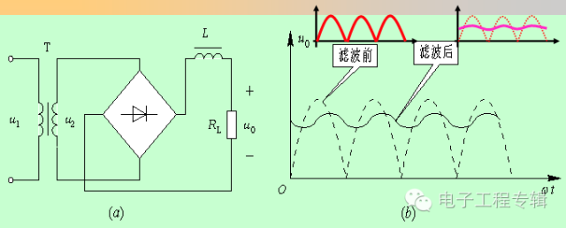
For the DC component: XL=0 is equivalent to a short circuit, and the voltage is mostly reduced to RL. For harmonic components: The higher f, the larger the XL and the lower the voltage on the XL. Therefore, a relatively smooth DC voltage is obtained at the output. When ignoring the DC resistance of the inductor, the average output voltage is about: UL=0.9U23.3, RC – pai type filter is used in the case of small current and low requirements, and the common resistor replaces the inductor L to form the RC-pai type. filter. It has low cost, small size and good filtering effect. However, since the resistor consumes power, the power loss of the power supply is large, and the efficiency of the power supply is lowered, which is generally suitable for occasions where the output current is small. 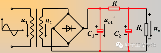
4, Zener diode 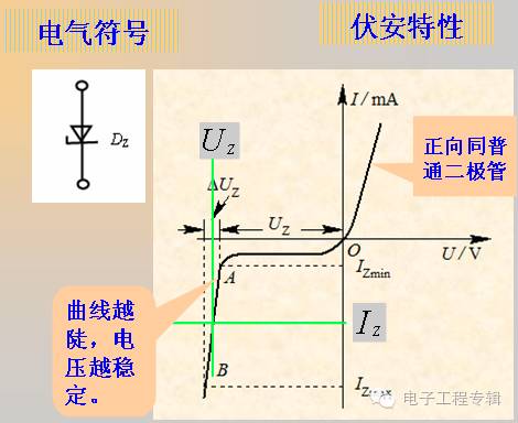
When the Zener diode operates in the reverse breakdown state, when the operating current Iz is between Izmax and Izmin, the voltage across it is approximately constant.
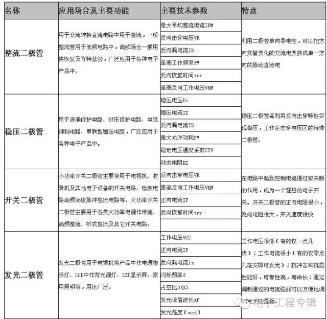
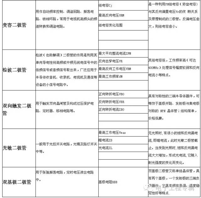
5, the classification of diodes
Asic Miner Bitmain:Asic Miner Bitmain Ka3 166Th Kda Mining Machine
Bitmain is the world's leading digital currency mining machine manufacturer. Its brand ANTMINER has maintained a long-term technological and market dominance in the industry, with customers covering more than 100 countries and regions. The company has subsidiaries in China, the United States, Singapore, Malaysia, Kazakhstan and other places.
Bitmain has a unique computing power efficiency ratio technology to provide the global blockchain network with outstanding computing power infrastructure and solutions. Since its establishment in 2013, ANTMINER BTC mining machine single computing power has increased by three orders of magnitude, while computing power efficiency ratio has decreased by two orders of magnitude. Bitmain's vision is to make the digital world a better place for mankind.
Asic Miner Bitmain,Ka3 166Th Kda,Kda Miner Antminer Ka3,Asic Miner Ka3,ka3 miner
Shenzhen YLHM Technology Co., Ltd. , https://www.asicminer-ylhm.com