Microprocessors and application specific integrated circuits (ASICs) require low voltage, high current power supplies. These power supplies typically have very stringent requirements on output voltage deviation, especially for load transient events. Testing designers for these power supplies can present many challenges and it is difficult to verify compliance with specific specifications.
This article answers questions related to load transient testing and describes some of the ways to simplify testing under harsh conditions.
In order to properly design the power supply, you first need to understand all the transient parameters and how they are applied to the test. Common transient parameters include:
• The size of the load step (expressed in amps or as a percentage of full load) • Minimum load in transient events (sometimes zero) • Rate of conversion of the load step (usually in amps per microsecond) • Order Maximum voltage deviation allowed by the poles • Estimated recovery time
Figure 1 illustrates how these specifications are usually defined.

Figure 1: Graphical description of load transient measurements.
Once you understand all the parameters, you can try to design a power supply that meets your requirements. However, testing according to the above requirements becomes a major challenge. The output voltage is 1V, the load step is 100A, and the conversion rate of 1000A/μs is not common. In most test cases, the limiting factor is the inductance between the power supply being tested and the load. In practical systems, the power supply tends to be close to the load it supplies, minimizing parasitic inductance.
There are several ways to test the load transient response of a selected power supply, but each method has its pros and cons. Here I will compare the following options: external electronic load, external transient board, field effect transistor (FET) Slammer, onboard transient generator and socket based transient tester.
External electronic loads may be the most common and convenient method of testing transient response. Most loads have modes that allow you to easily set the current level and conversion time. The main disadvantage due to external wiring or actual load limitations is the limited conversion rate.
External transient boards typically achieve better results in terms of slew rate, but this reduces some flexibility. Depending on the design, the load transient board may be limited by the maximum current, heat dissipation, or slew rate. Since transient boards are external connections, wiring is often the bottleneck for slew rate limiting. In addition, you need to adjust or configure the board for each test power supply.
The FET slammer is a fast and simple way to achieve high speed transient results. The metal oxide semiconductor field effect transistor is connected from the drain to the source through a resistor or directly through the output of the power supply, and the function generator controls the gate. Due to the small number of external wiring, the parasitic inductance is greatly reduced.
While this approach typically produces high slew rates, it can be difficult to control and repeat tests. It may be necessary to modify the PCB (Figure 2). Another problem with this approach is that it is difficult to measure the actual load step current and the measured data may be inaccurate.
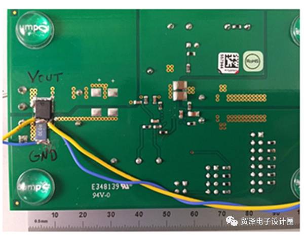
Figure 2: Example of a PCB with FET slammer.
When testing high current, high speed transient performance, the onboard transient generator is very practical and can be designed for specific load transient specifications. The main disadvantage is that the components add extra cost and space. In addition, taking multiple different measurements can be difficult or time consuming.
The design of the onboard transient generator is also very complex. It can be as simple as a 555 timer controlled resistor and FET, or as complex as the design shown in Figure 3. A more complex design uses multi-stage and smaller, faster switching FETs that achieve a conversion rate of 1000 A/μs.
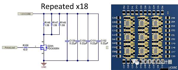
Figure 3: Complex version of the onboard transient generator.
The last option is to use a processor socket and a dedicated transient tester . This option is the most expensive method because the tool itself is expensive and the price of the PCB is increasing, but the most accurate results can be obtained for a given set of processor requirements. Processors or ASIC manufacturers often develop such tools, so these tools are designed to provide the right test conditions.
Table 1 summarizes several transient test methods.
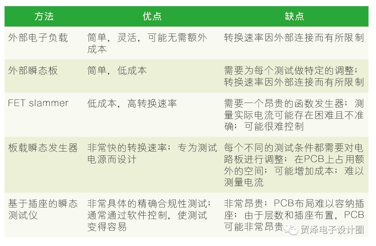
Table 1: Comparison of different transient test methods.
Load transient testing is a very important part of power supply design and compliance. Parasitic inductance in the test fixture can have a negative impact on the ability to achieve the desired slew rate. Using the above method can help to avoid this problem.
suzhou whaylan new energy technology co., ltd , https://www.whaylan.com