Xuebao Wang, Jiangsu Institute of Automation
Keywords: VPX; XMC; computer; high-speed serial
0 Preface
At present, VME64x can no longer meet the increasingly high performance requirements in the aviation field and applications in harsher environments. Many applications, such as radar, sonar, video image processing. Intelligent signal processing, etc., due to VME64x transmission bandwidth limitations, the system performance can not be further improved. There is an urgent need for a new bus that replaces the existing VME64x bus to increase system transmission bandwidth.
VPX bus is the natural evolution of VME technology. It uses high-speed serial bus instead of parallel bus as its main change. VPX uses modern industry-standard serial switching fabrics such as RapidIO and Advanced Switching Interconnect to support higher backplane bandwidth. These high-speed serial exchanges provide data transfer rates of 250 MBytes/sec per differential pair. If 4 channels are at the theoretical rate of 1 GBytes/see. The core exchange of VPX provides 32 differential pairs, forming four 4-channel ports, each of which is bidirectional (a transmit differential pair and a receive differential pair). The theoretical total bandwidth of the VPX module is 8 GB/sec.
In the VPX computer system, the peripheral function module is usually implemented by using a PMC/XMC carrier board and a module. The carrier board is a universal module that provides interface functions. The module is mainly to achieve various functional circuits. Different functions of PMC/XMC modules and carrier boards can be combined into VPX modules with different functions. Therefore, it is very meaningful to design the carrier board.
The bus of the carrier board module uses the PCI Express bus. One x8-wide PCI Express bus interface is brought out from the VPX. Because the PCI Express bus is a point-to-point connection and contains two PMC/XMC interfaces on the carrier board, it is necessary to expand the one-way interface to two. In order to realize this function, the PCI Express switching circuit needs to be implemented on the carrier board.
This article describes the design and implementation of a VPX-based PMC/XMC carrier board and the high-speed circuit design simulation process.
1 Design Principle
The carrier board is structurally designed with the VPX standard 6U board. The upstream interface of the carrier board is connected to the VPX connector. The carrier board can be inserted into the corresponding VPX slot. The two downstream interfaces of the board are respectively connected to the PMC/XMC connector to connect to the PMC/ XMC module.
As shown in Figure 1, the switch board uses the PEX8524 as the core, and all input and output signals revolve around the PEX8524 chip. The x8 PCI Express upstream interface signal splits through the PEX8524 to the 2-way X8 PCI Express downstream interface signal. This expands the PCI Express from the input single port to the two ports, which means that only one PCI Express device can be attached. The upstream interface (upstream) can be connected to two devices through the PEX8524.
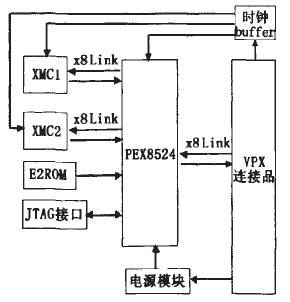
Figure 1 hardware block diagram
The host (host) can initiate operations such as configuration and read/write operations on the PEX8524 and devices attached to the downstream interface of the PEX8524 upstream 121 (upstream).
2 implementation methods
2.1 The main original device selection
The choice of switching chips depends on the system's requirements for port and channel resources. In the current use, there are 3 ports and 24 channels. Currently, existing products on the market generally design switch chips in proportion to port and channel ratio of one to four. The number of ports is growing at even-numbered levels, and there are four ports, six ports, eight ports, and twelve ports. So choose to use the 6-port switch chip.
Currently, the manufacturers of switching chips in the market mainly include PLX and Tundra. By contrast, PLX's products are relatively more focused on PCI and PCI Express. So choose to use PLX's 8-port chip PEX8524. The PEX8524 is a PLX-specific chip for PCI Express port expansion. It contains 24 channels and 6 ports. The PEX8524 can be configured in a flexible manner, and the optional configuration scheme is also very rich. The clock part uses ICS's ICS9DBl04BF as a clock buffer to expand one clock input into four clock outputs.
2.2 PCI Express Hardware Interface Implementation
Each PCI Express port includes two parts of signals, port control signals and communication signals. The port control signals include hot swap control signals, clock enable signals, power enable signals, and the like. The communication signal is mainly composed of LANe channels. Each LAN channel includes one pair of transmission and reception differential signals. The number of Lane channels included in each PCI Express port is scalable, that is, the number of LANe channels included is variable. In this board, there are 3 cases where each port contains x4, x8, and x16 lane channels. High-speed differential signals are transmitted on the lane channel, and the highest signal transmission speed on each signal differential pair can reach 2.5 Gbit/s. The lane channel interconnected between two devices needs to add a capacitor to isolate the DC signal. Consider the frequency of signal transmission. The size of the capacitor is generally 0402. The small size can reduce the series equivalent inductance of the capacitor to improve the use of the high-frequency signal area. Performance.
2.3 Clock Design
The transmitter periodically outputs data at a rate of 2.5 Gbit/s. The clock that implements this rate must be accurate within +/-300ppm of the center frequency. It allows a maximum of 1 clock every 1666 clocks. There are two ways for the device to obtain the clock input, using the board clock and using an external input clock. In this design, an external clock is used. If Spread Spectrum Clocking (SSC) is used, it is generally required that the transmitter and receiver on the link must use the same reference clock. SSC is a technique for slowly modulating the clock frequency so that the clock center frequency can be reduced. EMI radiation noise at the office. With the SSC, the radiated energy does not produce a 2.5 GHz noise spike because the radiated energy is scattered in a small frequency range around 2.5 GHz. In this design, one input clock signal is divided into four clock signals for synchronization by the clock buffer.
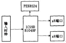
Figure 2 clock signal connection diagram
2.4 Power Design
PEX8524 chip needs to use 3 kinds of voltage, among them the core voltage is 1.0V, IO voltage is 3.3V, the serial transceiver power supply voltage is 1.2V, so need this board to offer three voltage sources of 3.3V, 1.2V and 1.0V .
Since this board does not have noise-sensitive analog circuits such as audio and RF, DC-DC circuits can be used to reduce power consumption. Compared with Linear Technology, National Semiconductor, Texas Instruments and other companies of the same type of voltage conversion chip, choose Texas Instruments PTH08T220W module as a 12V ~ 1.0V voltage conversion chip, select Texas Instruments PTH05010 as a 5V ~ 3.3V voltage conversion chip, select National Semiconductor LP3964 is a 3.3V to 1.2V voltage conversion chip. They have more than 90% conversion efficiency, simple peripheral circuits, smaller packages, and ripple voltages below 2.5%.
The PEX8524 chip has strict requirements for power-up and power-down sequencing. The order of power-on is 1.0V, 1.2V, and 3.3V, respectively. The order of power off is 3.3V, 1.2V, and 1.0V. Intersil's ISL6123 is used to control the power-up sequence of the PEX8524 chip. This chip controls the output power-up control signal time by connecting different values ​​of capacitors to the corresponding pins.
2.5 Reset Design
As shown in Figure 3, the external reset signal is used as the input of the logic gate together with the manual reset signal of the board after input, the output of the logic gate is connected to the reset control chip MAX6420, and the signal output from the MAX6420 is directly provided to the PEX8524 and each slot As a reset input.
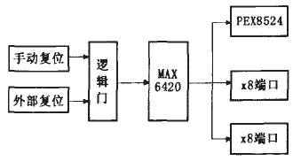
Figure 3 reset signal connection diagram
3 High Speed ​​Circuit Design
The design of the printed circuit board includes the PCI Express circuit design. The PCI Express bus signal is a high-speed signal. Therefore, the circuit design also belongs to the high-speed circuit design. If the design of the high-speed circuit PCB (printed circuit board) is to be successful, it must be At the beginning of the circuit design, simulation tools were used to verify the simulation. According to the feedback results of the simulation, the design was continuously modified. After the PCB was completed, the simulation results of the signal could be verified by high-speed oscilloscopes or high-speed logic analyzers. The modification of simulation parameters provides the basis for continuous improvement of high-speed circuit design in this closed-loop process.
High-speed signal simulation is the key to the design of this board and the core, PEX8524 chip external signal types and numbers are relatively small, there is no complex logic design in the periphery, just put some requirements on the clock and power, but the transmission on the PCB The signal quality of high-speed differential signals has high requirements. This problem is also a common problem faced by all current high-speed designs. There are many factors that need to be considered due to high-speed PCB design, such as medium, plane division, signal length, and so on. The traditional design criteria are no longer accurate, so you need to rely on simulation tools to provide design basis. The simulation tool used in this design is Mentor's Hyperlynx GHz. The Hspice simulation model is provided by the device manufacturer.
The simulation process mainly includes pre-simulation and post-emulation. The specific contents of the two simulations are described below.
3.1 The realization of the pre-simulation
Pre-simulation refers to the simulation performed before the PCB is completed, that is, the functional simulation. The main purpose is to verify the correctness of the principle design. Therefore, in this simulation process, only some basic parameters need to be set, and the parameters are compared and simulated. The results provide the basis for the design of the PCB and does not require the full information of the PCB to be imported.
(1) Simulation schematic drawing.
Performing pre-simulation in Hyperlynx environment requires drawing the principle network first.
As shown in Figure 4, the figure shows a typical PCI Express signal path. The figure basically includes all the elements contained in the PC]Express actual path transmission path. After the signal is sent out, it passes through the transmission line and then passes through the via twice to switch the signal transmission layer, and finally passes through the capacitor to receive.
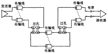
Figure 4 front simulation schematic
(2) Impedance control.
The PCI Express standard requires a 1000-hm differential impedance. Impedance is mainly determined by line width, line spacing, copper skin thickness, dielectric layer thickness, dielectric material, etc. The calculated interface of characteristic impedance is shown in Fig. 5. The calculated characteristic impedance is 94.50 hm, which meets the requirements.
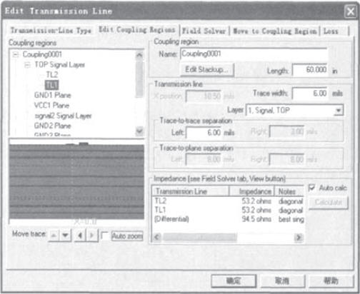
Figure 5 The characteristic impedance calculation interface
(3) Stack control.
As shown in FIG. 6 , the stack of printed circuit boards of the main module is the top layer (signal layer), the ground layer, the internal signal layer 1, the power layer, the ground layer, the internal signal layer 2, the ground layer, and the bottom layer (top layer) from top to bottom. Floor). In this distribution mode, each signal layer is adjacent to the ground. The formation can be used directly as a reference plane for the signal. There is a plane layer between any two signal layers to prevent interference between signal layers.
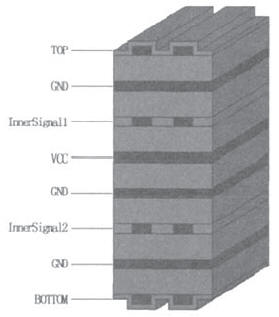
Figure 6 stack control chart
3.2 Post-emulation implementation
After the printed circuit design is completed, the circuit is imported into the Hyperlynx environment for post-emulation. The simulation results are shown in Fig. 7. It can be seen from the figure that the signal quality satisfies the requirements within the range that can be normally identified.
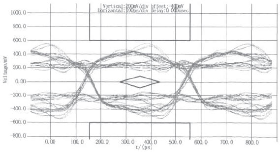
Figure 7 Eye diagram of the receiver
4 Conclusion
This design is compact in structure, stable in performance, strong in anti-interference, and suitable for various industrial control applications. The design has been applied many times in the industrial control environment and has been tested in different environments. After long-term evaluation, the module is stable and reliable.
With the development of technology, VPX computers will gradually replace the original parallel architecture computers in the field of industrial control and resistance to harsh environments. Therefore, the VPX-based XMC/PMC module will be used more and more.
Sanitation dispenser,it can automatically receive the signal to turn on the switch to the machine when the person reaches out the hand, so that the work sprays disinfectant or foam.
There are two working modes: automatic setting time and random time. It can be placed in toilets, kitchens, office buildings, hospitals, banks and other places.Suitable for a variety of viscous liquids, such as hand soap, detergent, disinfectant, sunscreen, etc. It can be placed in toilets, kitchens, office buildings, hospitals, banks and other places.

Sanitizer Dispenser,Hand Sterilizer Dispenser,Wall Mounted Hand Sanitizer,Automatic Hand Sanitizer Dispenser
Taishan Jie Da Electrical Co., Ltd , https://www.ts-jieda.com