Hardware system high reliability design
1 hardware circuit design
The hardware circuit principle is shown in Figure 1. In the specific design, each part should consider the anti-interference problem to minimize the impact of interference on the overall system performance, and ensure that the system has high enough reliability.
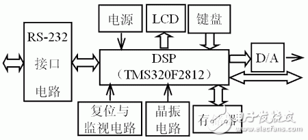
Figure 1 Intelligent controller hardware circuit block diagram
1DSP part
The controller is based on TI's TMS320F2812 (hereinafter referred to as F2812). It is a high-performance, multi-functional and cost-effective 32-bit fixed-point DSP chip dedicated to control. The circuit design of the F2812 part focuses on the following issues:
â— Power-on sequence. F2812 is a low-voltage, multi-power DSP. It must meet the order of I/O power supply before the CPU core power supply, and the power-on time difference between the two should not be too long (generally no more than 1s), otherwise it will affect the service life of the device or even damage. Device. This paper uses TPS75733KTT and TPS76801Q power chip to design the power module, which meets the special requirements of the above power-on sequence.
â— System clock. F2812 requires input clock signal level of 1.9V (at this time, the main frequency can reach up to 150MHz) or 1.8V (at this time, the highest frequency is 135MHz), while the output level of ordinary crystal oscillator is 5V or 3.3V, so it cannot be directly used. Crystal design system clock. In order to improve the stability and reliability of the overall system operation, this design uses a crystal and two capacitors and the F2812 on-chip clock module to form an oscillating circuit to meet the clock requirements.
â— Processing of unused input/output pins. Unused input pins should not be left unconnected. For critical control input pins (such as Ready and Hold), they should be fixed high or low. Non-critical input pins should be pulled up or pulled down. It is a fixed level; unused output pins can be left unconnected.
2 power section
This design takes the following measures for the DC side:
â— The power supply is separately powered by internal and external types, and technical measures such as isolation, filtering and grounding are adopted. The internal power supply is responsible for the power supply of the F2812 core system and has a voltage monitor for power supply abnormal protection; the external power supply only contacts the external interface.
â— The analog power supply is separated from the digital power supply and powered by separate power supplies.
â— A two-stage voltage regulation method is adopted for the rectified DC voltage to ensure that the pre-stage voltage regulator can still output the specified voltage after being affected.
3 input and output channel section
The input and output channels are connected to the process, which is the main channel for the process interference to enter the DSP system, and is also one of the important contents of the anti-interference design of the DSP system. The anti-interference design of the input and output channels mainly adopts isolation measures, which can greatly improve the signal-to-noise ratio on the process channel.
4 communication part
The F2812 chip has two serial communication interfaces, which can be freely configured as standard serial port RS-232 or RS-485 according to specific needs. This design uses RS-232, and in order to improve the anti-interference ability of the whole system, the high anti-interference driving chip MAX3160 is selected and isolated by high-speed optocoupler.
2 PCB circuit board design and production
At present, electronic devices are generally assembled using PCB boards. With the rapid development of integrated circuits and related technologies, the density of components on PCBs is getting higher and higher, and the quality of PCB design and fabrication has an increasing influence on the reliability of DSP systems. Therefore, when designing and fabricating PCBs, not only the layout of components and circuits, but also the relevant anti-interference design rules should be considered.
1PCB layout
PCB layout is very important. It not only determines the visual effect of the board and the routing rate of the automatic wiring, but more importantly, it affects the overall performance of the instrument. Therefore, the layout must be considered comprehensively and follow certain rules, including:
â— The geometrical dimensions of the PCB board should be appropriate. If the size is too large, the line impedance will be increased to reduce the noise resistance. If the size is too small, the heat dissipation will be affected, and adjacent lines are susceptible to interference.
â— The components and signals should be properly partitioned to separate the strong and weak signals. The digital and analog signals are separated, and the interference source is separated from the sensitive components.
â— Position the function modules as much as possible according to the signal flow to make the signal directions consistent;
â— Perform component layout centering on the core components of each functional module, and consider component arrangement and soldering, not too dense;
2PCB wiring
In the PCB design process, the wiring work is very skillful and is a very important step. The following rules should be followed when wiring:
â— The wiring direction of two adjacent layers should be as vertical as possible, and if necessary, ground wire can be isolated;
â— Ground and power lines should be as thick as possible to reduce voltage drop and reduce coupling noise;
â— The frequency of the digital circuit is high, and the sensitivity of the analog circuit is strong. When wiring, the analog device should be kept away from the digital signal line as much as possible, and the digital area and the analog area should be isolated by the ground line;
â— The entire PCB board has only one ground node externally. In the PCB board, the digital ground and the analog ground are separated. Usually, the digital ground and analog ground can be connected together at the analog ground pins of the D/A converter. ;
3 power cord design
The solution to the interference problem is to separate the devices in the power supply unit separately, and then completely isolate the other parts with the thick and thick ground lines, and then place bypass capacitors and decoupling capacitors near the power device to maximize Ground to reduce interference on the output power line. In addition, according to the size of the current, the power line should be widened as much as possible, and the direction of the power line and the ground line should be consistent with the data transmission direction as much as possible to improve the anti-noise capability of the system.
4 ground line design
The noise and interference of electronic systems are closely related to their grounding methods. Good grounding often solves most of the interference problems.
For low-frequency circuits, the influence of inductance between wiring and components is relatively small, and the circulation formed by the grounding circuit has a large influence on interference. In this case, a grounding method should be adopted to minimize the potential difference on the ground line; In high-frequency circuits, the ground line impedance will become very large. At this time, shortening the length of the ground line to reduce the ground line impedance becomes a key issue, so the nearest multi-point grounding method should be adopted. In addition, the grounding wire should be thickened as much as possible to reduce the grounding resistance. Otherwise, the signal level will be unstable due to the change of the grounding potential, thus reducing the noise immunity.
5 filter capacitor design
The capacitance of luF~l0uF is connected between the power line and the ground line at the entrance of the circuit board, which can effectively eliminate low frequency interference. For high-frequency interference signals, 0.01μF and 0.1μF capacitors can be placed next to the power and ground pins, especially to directly connect 0.1μF high frequency between the power and ground lines of each integrated circuit chip. capacitance. In addition, ferrite beads can also be used for high-frequency filtering, which can be equivalent to a series connection of a resistor and an inductor. The AC impedance at high frequencies is large, while the DC impedance is small (close to 0 Ω). In this way, the high frequency interference signal is absorbed and consumed as heat.
The GFCI will not protect you from line contact hazards (i.e. a person holding two "hot" wires, a hot and a neutral wire in each hand, or contacting an overhead power line). However, it protects against the most common form of electrical shock hazard, the ground-fault. It also protects against fires, overheating, and destruction of wire insulation.
Ground Fault Circuit Interrupter UL
Ground Fault Circuit Interrupter UL,Auto-Monitoring Ground Fault Circuit Interrupters,Ground Fault Circuit Interrupter,Outlet Ground Fault Circuit Interrupter
Hoojet Electric Appliance Co.,Ltd , https://www.hoojetgfci.com