It is critical to address noise and interference issues from the very beginning of the design. For the first time, many designs did not pass the Federal Communications Commission (FCC) EMC test. If you spend some time on low-noise and low-interference design methods in your early designs, you will reduce the delay in re-design costs and time-to-market for subsequent phases. Therefore, from the very beginning of design, development engineers should focus on:
1. Use a power supply with low switching noise under dynamic load conditions;
2. Minimize crosstalk between high-speed signal lines;
3. High frequency and low frequency decoupling;
4. Excellent signal integrity with minimal transmission line effects;
If these goals are achieved, the development engineer can effectively avoid the noise and EMI defects.
Noise impact and control
For high-speed DSPs, reducing noise is one of the most important design criteria. Excessive noise from any noise source can cause random logic and phase-locked loop (PLL) failures, reducing reliability. It also causes radiated interference that affects the FCC certification test. In addition, debugging a very noisy system is extremely difficult; therefore, eliminating noise—if it can be eliminated altogether— requires a lot of effort in board design.
In audio and video systems, even relatively small interference can have a significant impact on the performance of the final product. For example, in an audio capture and playback system, the performance will depend on the quality of the audio codecs used, the power supply noise, the PCB layout quality, and the crosstalk between adjacent circuits. Moreover, the stability of the sampling clock is also required to be very high to avoid undesired noise such as "click" and "click" during playback and capture.
In the video system, the main challenge is to eliminate color distortion, 60Hz "click" and audio knocking. These are all harmful to high quality video systems, such as security monitoring applications. In fact, these problems are usually related to poor design of the video circuit board. Specifically, power supply noise is transmitted to the DAC output of the video; audio playback causes transients in the power supply; the audio signal is coupled to a signal line of a high-impedance video circuit.
These typical sources of video problems include: overshoot and undershoot of synchronization and pixel clocks; jitter affecting color coding and decoding and pixel clocking; image distortion in the absence of termination resistors; flicker caused by poor audio and video isolation.
The noise interference problems that are easily generated by audio and video applications are also common to all communication systems that require very low bit error rates. In communication systems, radiation not only generates EMI problems, it also blocks other communication channels, causing spurious channel detection. These challenges can be overcome with appropriate board design techniques, shielding techniques, and isolation of RF and mixed analog/digital signals.
There are many potential switching noise sources in high-speed DSP systems, including: crosstalk between signal lines; reflection due to transmission line effects; voltage drop due to inappropriate decoupling capacitors; high-inductance power lines, oscillators, and phase-locked loops Circuits; switching power supplies; large capacitive loads caused by linear regulator instability; disk drives.
These problems are produced jointly by electrical coupling and magnetic coupling. The electrical coupling is caused by the parasitic capacitance and mutual inductance of adjacent signals and circuits, and the magnetic coupling is caused by the adjacent signal lines forming a radiating antenna. If radiation interference is strong enough, it will cause EMI problems that can destroy other systems.
When noise in a high-speed DSP system cannot be eliminated at all, it should be minimized. There are noises inside the electronic components. Therefore, careful selection of device characteristics and selection of appropriate devices are critical. In addition to the correct choice of devices, there are two general techniques, namely PCB routing and loop decoupling can help control system noise. A good PCB layout will reduce the possibility of noise channels. In addition, the radiation that can be transmitted to the printed lines and the current loop is reduced, and the decoupling prevents the influence of noise generated by the adjacent circuits. The best way is to filter out the noise from the source, but it can also make the adjacent circuit insensitive to noise or eliminate the noise coupling channel.
Now we discuss several techniques that can solve many common problems caused by system noise and EMI.
Keep the current loop short
The low-speed signal current has the smallest impedance along the shortest path back to the source. The high-speed signal is returned along the smallest path of the inductor: this smallest loop area is below the signal line, as shown in Figure 1.
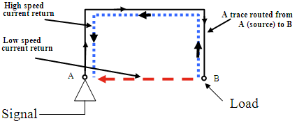
Figure 1: Comparison of high-speed signal and low-speed signal current
Therefore, one of the goals of high-speed signal design is to provide a minimal inductance loop for the signal current. This can be achieved using power planes and ground planes. The power plane minimizes parasitic inductance by forming natural high-frequency decoupling capacitors. The ground plane forms a shield plane, known as the mirror plane, which provides the shortest current loop.
An effective PCB layout method is to tie the power plane and the ground plane together. This creates a high plate capacitance and low impedance, which helps to reduce noise and radiation. For shielding, the best choice is: The key signal is best placed close to the ground plane, while the rest should be close to the power plane side.
In high-speed video systems, keeping the loop short means that the video ground cannot be isolated. The audio ground that must be isolated must not be short-circuited to the digital ground at the data entry point, as shown in Figure 2.
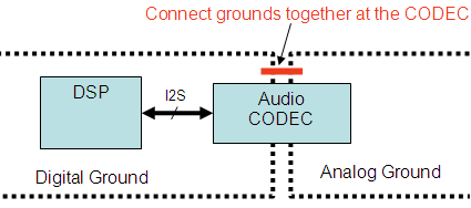
Figure 2: Audio isolation
Power isolation and phase-locked loop
How to achieve the best power supply is the biggest challenge to control noise and radiation. The dynamic load switching environment is very complex and includes the following factors: entering and exiting low power modes; large transient currents caused by bus competition and capacitor charging; large voltage drops due to unreasonable decoupling and wiring; The oscillator overloads the linear regulator output.
Figure 3 shows an example of a design current loop where power line decoupling is used. The decoupling capacitor in this example is as close to the DSP as possible. If there is no decoupling, the dynamic current loop will be large, which will increase the drop in the power supply voltage and generate electromagnetic radiation.

Figure 3: Power Decoupling
When powering the PLL, power isolation is very important because the PLL is very sensitive to noise and requires very low jitter for a stable system. You also need to choose analog or digital PLLs. Analog PLLs are less sensitive to noise than digital PLLs.
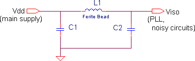
Figure 4: PLL power isolation
The âˆ-type filter with low cut-off frequency as shown in Figure 4 is often used to isolate the PLL from other high-speed circuits in the system. A better approach is to use a low-dropout (LDO) voltage regulator to independently generate the PLL's supply voltage, as shown in Figure 5. Although this method increases the cost, it ensures low noise and excellent PLL performance.
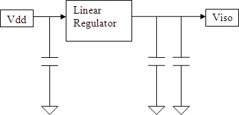
Figure 5: LDO Isolation Using LDOs
Crosstalk and transmission line effects
Interference between signals, that is, crosstalk, can be transmitted between printed lines by electromagnetic radiation. This may also be generated electrically from unwanted signals on the power supply and ground planes. Crosstalk is inversely proportional to the square of the trace spacing. Therefore, to minimize crosstalk, the wiring spacing of single-ended signals should be at least 2 times the width of the traces. For differential signals such as Ethernet and USB, the trace pitch needs to be the same as the trace width in order to match the differential impedance. The key signal can be shielded by the ground and the power plane, or the ground line parallel to the signal can be added when the board is changed.
Some signals also generate high-frequency harmonics that cause crosstalk. Since the energy of the radiation is proportional to the rise and fall times of the signal, the slower rise or fall time will cause less interference. Figure 6 shows examples of video interference that may be caused by the radiation of the internal clock. In the North American second channel, the third harmonic of the 18.432 MHz audio clock will produce the interference shown on the left in the figure. By adding a series resistor to the audio clock trace to slow down the rise and fall times of the clock, the interference is reduced. The result is shown on the right side of Figure 6. However, designers need to understand timing margins in order to reduce the rising and falling edges to the limits allowed by the system.

Figure 6: Solve audio and video crosstalk
Associated with crosstalk is the transmission line effect, which occurs when a high-speed printed line becomes a transmitter that produces radiated interference. In general, the printed line transmits signals when the rise time of the signal is less than 2 times the propagation delay. This implies an experience that the length of the printed lines should be as short as possible in order to reduce the propagation delay. The other is that reasonable signal termination will slow down the rise time of the signal, thereby minimizing overshoot and undershoot caused by reflections. Figure 7 shows how to use parallel termination to correct the level and minimize transmission line effects.
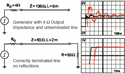
Figure 7: Using Termination to Minimize Transmission Line Effect
The designer may question whether it is still important to externally connect the load resistors since the resistors are already integrated inside the chip. In fact, in addition to controlling the effects of transmission lines, external resistors can also enable precise adjustment of signal integrity. The DSP cannot match the circuit board impedance perfectly, so terminating the load can reduce the source current, as well as the rise and fall times.
As with external termination load resistors, external pull-up and pull-down resistors are also important. For unconnected pins, although the internal pull-up and pull-down resistors are sufficient, high-speed switching noise can be transmitted and the internal logic on the connection can be triggered by mistake.
Control EMI
Radiation that can be emitted outside the system is considered EMI, which may make the design fail FCC certification. There are two possible types of radiation: one is that the emission source is a straight type signal trace, or the common mode radiation of the cable, and the other is differential mode radiation whose signals and loops form a large current loop. Common mode radiation decreases with increasing frequency, while differential mode radiation increases with frequency until it reaches its saturation point. The radiation of these two modes is shown in Figures 8 and 9.

Figure 8: Common mode radiation
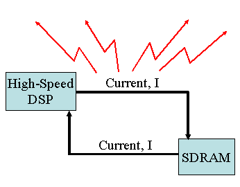
Figure 9: Differential Mode Radiation
How to deal with EMI depends on the source of radiation. For common-mode radiation, a choke can be added to the cable when the EMI comes from an external cable (as shown in Figure 8). If the EMI is caused by an internal transmission line, it is usually used to terminate the load, but adding a ground line between the signal lines also helps reduce radiation. Another possible solution is to shorten the trace length of the signal to less than 1/20 of the signal wavelength (or the reciprocal of the signal frequency). For example, to avoid transmission of radiation, a 500-MHz trace should be shorter than 1.18 inches.
For differential mode radiation, the radiated energy is a function of current, loop area, and frequency. Methods of reducing radiation include terminating the load to reduce the source current, providing a suitable current path to provide a circuit that reduces the loop area, or reducing the frequency.
When calculating the decoupling resistance, dynamic currents should also be considered. High-speed currents can change at any time, and this transient can also cause radiation. In addition, the self-resonance limiting frequency range should be prevented when changing the value of the capacitor. PCB layering is a good solution because the power plane naturally decouples the high frequencies and the ground plane provides the shortest loop. Separate high-speed signals and keep them away from other signals. If possible, do not separate the formation. Although noise and radiation are caused by the complex uselessness of the system design, they can be controlled by some of the simple methods described above.
This article summary
There are many potential sources of noise and radiation in high-speed DSP video systems that can disrupt the operation of the system or make the design pass the FCC certification. Fortunately, the planning and mastery of noise and radiation can help system designers minimize these problems. Early efforts will save a lot of debugging work and late troubles. PCB layout and loop decoupling are two common techniques designers can use to limit system noise and EMI. With these technologies, DSP video designers can effectively solve system noise and radiation.
Babbitt Wire is with tin as the base, the product is added with certain amount of antimony, copper
or other improved elements.
Sn Sb7Cu3 Babbit metal is suitable for metal spraying on the end face of metalized ï¬lm capacitor. With strong adhesive force, good weldability and low loss angle, it is an ideal metal spraying material for laminated capacitor.
Other trade marks are suitable to use CMT, TIG and MIG technology to manufacture sliding bearing bush material layer. It is of high bonding strength with substrate, with material utilization rate of 70~80%. It has small amount of ingredient segregation without any loose or slag inclusion. The internal control standard of the alloy composition is prevailing over GB/T8740-2013. Babbi1 metal added with improved elements can substantially enhance the service life.
Snsbcu Babbitt Wire,Overlaying Materials,Thermal Spray Babbitt Wire,Babbitt Wire
Shaoxing Tianlong Tin Materials Co.,Ltd. , https://www.tianlongspray.com