One of the key benefits of FPGA-based prototyping is that it allows embedded software to run immediately once the first SoC chip is in the lab. This early access gives development teams a head start, enabling them to begin testing and debugging much earlier in the design cycle.
As advocates of FPGA-based prototyping, we are not blind to its limitations. In fact, our "FPGA-Based Prototype Method Manual" aims to provide a balanced view of both the advantages and challenges of this approach. Our goal is not to discourage others from using alternative methods—such as System C-based virtual prototypes—but rather to ensure that those who choose FPGA-based prototyping understand the full scope of what they're getting into. After all, every method has its place, and the right choice depends on the specific needs of the project.
To make the most of this method, it's essential to clearly define the purpose and constraints of the prototype. Understanding these factors helps in making informed decisions about platform selection, IP reuse, design export, and debugging strategies. By studying real-world examples from other teams, we can learn from their successes and mistakes, ultimately improving our own processes.
FPGA-based Prototypes Can Meet Diverse Needs
Prototyping isn’t just a simple process—it requires careful planning, execution, and reflection at every stage. Beyond explaining the tasks and skills involved, it’s also important to address the rationale behind choosing FPGA-based prototyping over other methods. A common question among prototype designers is, “Why are you doing this?†The answers vary widely, but we’ve categorized them in Table 1 to help clarify the main motivations.
For instance, one team might be prototyping to test how a system performs in a real-world environment, such as verifying compliance with a new interface standard. In such cases, an FPGA-based prototype offers the fastest and most accurate way to simulate real conditions before the actual chip is ready. This kind of early validation is crucial for identifying and fixing issues early in the development cycle.
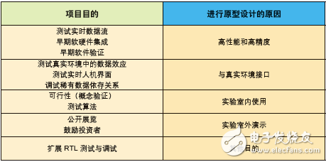
Table 1: Common purposes and reasons for using FPGA-based prototypes
By understanding the goals behind each prototype, we can better determine whether FPGA-based prototyping is the right fit for our own projects. Let’s take a closer look at the reasons listed in Table 1 and explore how FPGA-based prototyping can support these objectives. We’ll also share real-world examples and acknowledge the contributions of those who have helped shape this field through their experience and guidance.
High Performance and Accuracy
One of the primary reasons teams choose FPGA-based prototyping is the high performance and accuracy it provides. While there are many reasons for building a prototype, this is often the most fundamental. For example, a team may want to validate embedded software for a particular SoC and run it at full speed on real hardware. The underlying motivation is to ensure that the system performs reliably and accurately, something that can only be fully verified with real RTL.
Real-Time Data Streams
Another major advantage of FPGA-based prototyping is its ability to handle real-time data streams. SoCs are complex systems that depend on numerous variables, including previous states, input sequences, and system feedback. Connecting the SoC design to the rest of the system and running it at real-time speed allows developers to observe changes and responses instantly.
A great example comes from the HDMI prototype developed by Synopsys’ IP team in Porto, Portugal. In this case, HD media data is streamed through the prototype to a display, as shown in Figure 1. The block diagram illustrates how real-time audio and video data is received, processed, and output via the HDMI PHY connected to an external monitor. This real-time capability is only possible with FPGA-based prototyping, offering significant benefits for multimedia applications and any system requiring real-time input processing.
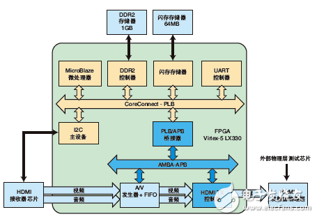
Figure 1: HDMI prototype block diagram
Software and Hardware Integration
In the example above, you may have noticed that the prototype uses a small MicroBlazeâ„¢ CPU along with peripherals and memory to represent the core components of an SoC. The software running on the CPU is used to load and control the A/V processing. However, in many SoC designs, the software is the most resource-intensive part of the system. By integrating hardware and software early in the development cycle, teams can identify bottlenecks, optimize performance, and ensure seamless interaction between different components.
SC/APC Fiber Optic Fast Connector
Sc/Apc Fiber Optic Fast Connector,Fiber Optic Adaptor Fast Connector,Fiber Quick Connect Kit,Sc Fiber Optic Fast Connector
Ningbo Fengwei Communication Technology Co., Ltd , https://www.fengweicommunication.com